Core identity and what the 50 MHz clock buys you
The MC860ENCVR50D4R2 is a single-core 32-bit PowerPC processor from the MPC8xx family, clocked at 50 MHz. That clock rate sets the instruction throughput ceiling — for a control-loop or protocol-conversion task, the core can sustain roughly one instruction per cycle on simple arithmetic, so the real-world packet-processing rate depends on how much work the CPM offloads. The headline I/O is four 10 Mbps Ethernet MACs — each port runs at 10BASE-T full-duplex. This part is built for multi-port bridging or protocol-gateway designs where the aggregate throughput stays under 40 Mbps and the CPM handles the MAC-level framing, leaving the core free for application code.
CPM co-processor — what it offloads and why it matters
The Communications Processor Module (CPM) is a dedicated RISC engine that handles HDLC, UART, SPI, I²C, IrDA, TDM, and PCMCIA in hardware. Without it, the main core would spend most of its cycles bit-banging serial protocols; with it, the 50 MHz core can dedicate its bandwidth to application logic, protocol translation, or network-stack processing. The DRAM controller supports standard SDRAM or EDO DRAM — no DDR or SDRAM-specific timing wizardry. The memory bus width and speed are set by the controller's own timing registers, not by the core clock, so the memory subsystem can run at a different rate than the 50 MHz core.
Package, temperature grade, and board integration
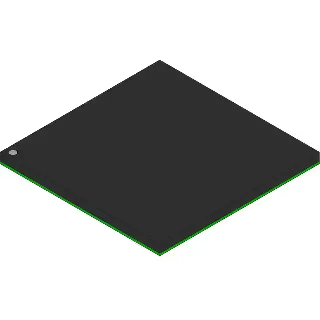
Housed in a 357-ball PBGA (25x25 mm body), the 1.27 mm ball pitch is a standard four-layer-board-friendly footprint — no microvia or HDI stack-up required. The supplier device package is 357-PBGA (25x25), and the mounting is surface-mount only. Rated for -40°C to 95°C ambient, this part fits outdoor telecom cabinets, factory-floor controllers, and engine-bay gateways without forced-air cooling. The 3.3 V I/O rail is shared across all peripheral interfaces, so level translation is needed only when connecting to 5 V legacy logic or 1.8 V modern memory.
How it compares to the 66 MHz sibling
The closest peer in the MPC8xx family is the MPC862PCVR66B, which runs at 66 MHz and adds a single 10/100 Mbps Ethernet port alongside the four 10 Mbps ports. The 50 MHz part is the cost-optimized choice for designs that never need Fast Ethernet and can live with the lower core clock — the 66 MHz sibling is the upgrade path if throughput requirements grow. Both parts share the same 357-ball PBGA footprint, the same 3.3 V I/O, the same CPM co-processor, and the same DRAM controller. A board laid out for the 66 MHz part will accept the 50 MHz part without a PCB spin, provided the firmware is built for the slower core clock.