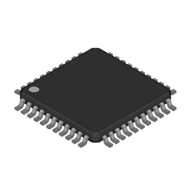
8-bit HC08 with USB — still a viable through-hole MCU
The NXP MC68HC908BD48IB-FR is an 8-bit microcontroller built around the HC08 core, running at 6 MHz with 48 KB of on-chip Flash program memory and 1K x 8 of RAM. It is the through-hole variant in a 42-pin SDIP (0.600" body width) — also listed as a 42-PDIP — which makes it one of the few remaining USB-capable MCUs in a DIP footprint that survives a wave-solder profile without a bake step, provided you respect the MSL. Its key differentiator is integrated USB 1.1 connectivity alongside I²C, a 6-channel 8-bit ADC, and a PWM peripheral with POR.
Flash memory and RAM — sizing the firmware budget
With 48 KB of Flash (48K x 8) and 1 KB of RAM, this part fits a USB HID-class or simple CDC-class device with a moderate application layer. The 1K x 8 RAM is the tighter resource — a 512-byte USB buffer plus a 256-byte stack leaves roughly 256 bytes for global variables. Firmware that streams data through double-buffered endpoints will need to manage the buffer pool carefully. The 6 MHz core clock limits throughput to about 1.5 MIPS (HC08 averages ~0.25 cycles per instruction). That is enough for polling a few ADC channels and servicing USB control transfers at full speed, but not for heavy DSP or real-time bit-banged protocols on all 32 I/O lines simultaneously.
Package and board-fit — through-hole with a 0.600" body
The 42-PDIP designation means the same mechanical outline; the plastic DIP body is 52.5 mm long and sits 4.5 mm above the board after wave solder. No exposed thermal pad, so all heat dissipation is through the leads — keep the ambient below 70 °C for reliable operation. RoHS non-compliant per the lifecycle record, so the solder joints use tin-lead finish. If your reflow or wave line is RoHS-only (lead-free solder), this part requires a segregated process or a waiver — verify your assembly house's policy before committing the BOM.
Lifecycle and supply — active but niche
It is not a high-volume commodity MCU — expect longer lead times and minimum order quantities typical of a mature, low-volume DIP package.