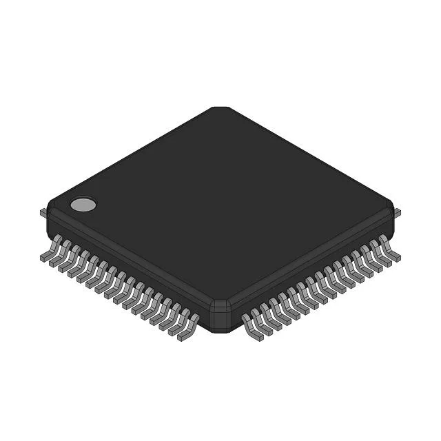
The NXP MC68HC11E0FU is an 8-bit microcontroller built around the M68HC11 CPU core, running at 2 MHz. It is a ROMless device — there is no on-chip program memory — so the firmware must reside in an external ROM, EPROM, or Flash memory connected via the external bus. The part includes 16 general-purpose I/O lines, an SCI and SPI serial interface, an 8-channel 8-bit ADC, a power-on reset (POR) and watchdog timer (WDT), and an internal oscillator. It is supplied at 3 V and comes in a 64-pin PQFP package for surface-mount assembly. Typical applications include industrial control, embedded instrumentation, and automotive body electronics where a mature, well-documented 8-bit architecture is preferred.
ROMless design — planning the external memory
Because the MC68HC11E0FU has no internal program memory, the BOM must include an external memory device — typically a parallel EPROM, OTP ROM, or Flash — plus address latches and decoding logic. The external bus interface is part of the M68HC11 architecture, so the memory map and chip-select logic need to be designed from scratch. This adds board area and component count compared to a masked-ROM or Flash-based MCU, but it gives flexibility in firmware updates (if Flash is used) and avoids NRE for mask ROMs in low-to-medium volumes.