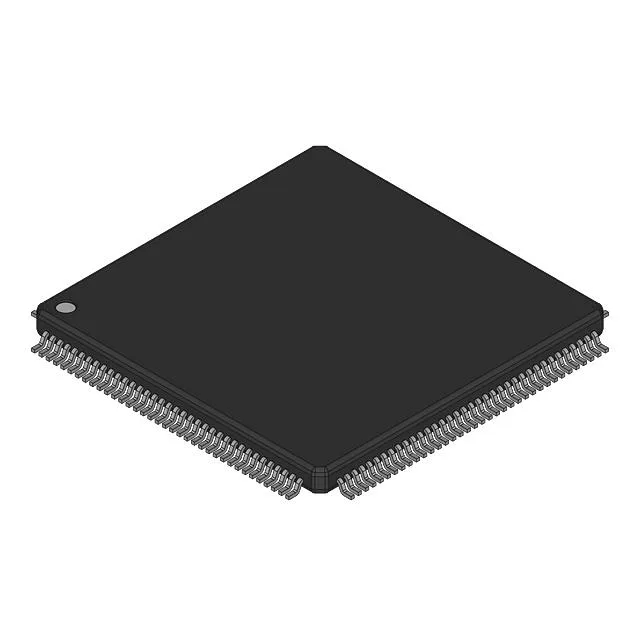
The NXP MC68332GCAG16 is a 32-bit single-core microcontroller built around the CPU32 core, clocked at 16 MHz. It is a ROMless device — all program code must reside in external memory accessed through the external bus interface (EBI/EMI). On-chip RAM is limited to 2K x 8, so data buffering or working memory also typically requires external SRAM or careful register usage. The part is supplied from 4.5 V to 5.5 V and rated over the industrial temperature range of -40°C to 85°C, making it suitable for factory automation, motor drives, outdoor telecom, and other environments where extended temperature is required but mil-spec qualification is not. The 144-LQFP package (20x20 mm body) is a surface-mount footprint that demands a standard reflow profile; no socket option is offered.
On-chip peripherals include a power-on reset (POR), a pulse-width modulator (PWM), and a watchdog timer (WDT).
Because the MC68332GCAG16 has no internal program memory (ROMless), every design must budget for an external non-volatile memory device — typically a parallel NOR Flash or an OTP EPROM — connected via the EBI. This adds PCB area, a second supply chain line, and a programming step during board assembly. It also means firmware updates require the external memory to be reprogrammable or socketed. For designs where code is fixed at the factory, a one-time-programmable EPROM is an option; for field-updatable systems, a Flash device is the practical choice. The small 2K x 8 on-chip RAM handles stack and small data structures; larger data buffers will need external SRAM.