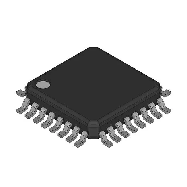
NXP Semiconductors MC100ES6111FAR2 — Discrete Semiconductors

NXP MC100ES6111FAR2 Fanout Buffer, 2:10, 2.7 GHz, 32-LQFP

MPNMC100ES6111FAR2
End of Life

NXP Semiconductors 100ES series Fanout Buffer (Distribution), Multiplexer, MC100ES6111FAR2, 2:10 ratio, 2.7 GHz max, differential I/O, 32-LQFP (7x7 mm), surface mount.

$7.33Ref. price · indicative, final on quote
Packaging32-LQFP
RoHSRoHS non-compliant
Series100ES
Sourced new & surplus through independent channelsAuthenticity-screened · ESD-safe packingListing updated Aug 2026

Specifications

MC100ES6111FAR2 specifications
ParameterValue
TypeFanout Buffer (Distribution), Multiplexer
Series100ES
MountingSurface Mount
Voltage2.375V ~ 3.465V
Frequency2.7 GHz
Operating temperature-40°C ~ 110°C
InputECL, HSTL, PECL
OutputECL, PECL
PackageBulk
Case32-LQFP
Number of circuits1
Ratio - Input:Output2:10
Differential - Input:OutputYes/Yes

Product details

2:10 fanout at 2.7 GHz — clock-tree fit

The MC100ES6111FAR2 is a 2:10 fanout buffer with an integrated multiplexer on the input side — one of two selectable clock sources fans to ten differential outputs. The 2.7 GHz maximum frequency covers the full range of 10G Ethernet reference clocks, FPGA transceiver reference oscillators, and SERDES PLL distribution. Differential input and output paths (Yes/Yes per the spec) reject common-mode noise coupled onto the clock traces between the source and the buffer, which is the dominant jitter mechanism on densely routed boards above 1 GHz.

Supply range and signal compatibility

Inputs accept ECL, HSTL, or PECL levels — a single device bridges between a PECL oscillator and an ECL-terminated fanout tree. Outputs are ECL or PECL, which require external termination resistors (typically Thevenin to VCC-2 V) rather than the series-source termination used for LVCMOS. The 32-LQFP (7x7 mm) package keeps the trace length from the output pin to the termination pair short enough to avoid stub reflections at 2.7 GHz.

Temperature grade and lifecycle

Note the RoHS compliance status: listed as RoHS non-compliant. This indicates a legacy lead-bearing solder finish (typically SnPb or AuSn). The part is still manufacturable and orderable, but the finish requires a Pb-compatible soldering profile — not a problem for mixed-technology assembly lines that maintain a SnPb reflow zone for legacy BOMs.

Frequently asked questions

What is the MC100ES6111FAR2 used for?

It is a 2:10 fanout buffer with a multiplexed input, designed to distribute a high-frequency clock from one of two sources to ten differential outputs with low additive jitter. Typical applications include SERDES reference clock trees, FPGA transceiver clock distribution, and telecom line-card timing.

Can I order MC100ES6111FAR2 through this distributor?

Yes.

What is the closest functional alternative to MC100ES6111FAR2?

The MC100ES6226FA is a sibling in the same 100ES series. It is a 1:9 fanout buffer with a divider, outputting LVCMOS or LVPECL rather than ECL/PECL. The MC100ES6111FAR2 has a 2:10 ratio and no divider — they are not pin-compatible and serve different fanout topologies.