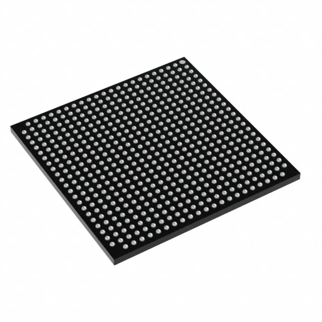
NXP Semiconductors LS1021ASE7KQB — Discrete Semiconductors
Technical Documents PDF / CAD
RoHS Compliant · Lead-Free EIA-481 Standard
NXP Semiconductors / Discrete Semiconductors

NXP LS1021ASE7KQB QorIQ Layerscape SoC, 1.0 GHz, Dual Core

MPN LS1021ASE7KQB
End of Life Spot Stock · 24-48h Dispatch 100% Original Sealed

NXP Semiconductors QorIQ® Layerscape LS1021ASE7KQB, 1.0 GHz dual-core ARM® Cortex®-A7 SoC, USB 3.0, SATA 6Gbps, triple GbE, DDR3L/DDR4, 525-FCPBGA.

In Stock: 635 pcs
MOQ: 1 pcs
Logistics: DHL / FedEx DAP (Global Express · 3-7d) Russia & CIS DDP (Door-to-Door Cleared)
Dispatch: Shenzhen / HK
Unit Price (USD)
$65.82 / pc
Direct Purchase Ready
Volume Pricing Breaks Confirmed upon quotation
1+ pcs
$65.82
10+ pcs
$59.24
30+ pcs
$53.97
100+ pcs
$48.71
500+ pcs
$45.42
Working on a production BOM or have a target unit price? Submit Target Price
Buy Now

$65.82 / ea

635 in stock — maximum per order · 3–4 days lead time

$59.24 / ea from 10 pcs

Upload Full BOM List
[SPEC] Essential Parameters Snapshot Full Specifications (14)
Package / Case 525-FBGA, FCBGA
Speed / Frequency 1.0GHz

Full Technical Specifications

14 Parameters
LS1021ASE7KQB specifications
Parameter / AttributeSpecification / Value
SeriesQorIQ® Layerscape
MountingSurface Mount
Display & interface controllers2D-ACE
Operating temperature0°C ~ 105°C
Number of cores (Bus width)2 Core, 32-Bit
USBUSB 3.0 (1) + PHY
SATASATA 6Gbps (1)
Speed1.0GHz
PackageTray
EthernetGbE (3)
Core processorARM® Cortex®-A7
Case525-FBGA, FCBGA
RAM controllersDDR3L, DDR4
Security featuresSecure Boot, TrustZone®
Series Sibling Variants

NXP Semiconductors QorIQ® Layerscape Series Models

Sibling variants, package options, and speed/density grades in this NXP Semiconductors semiconductor series. Active Shenzhen warehouse allocation and rapid 24-48h dispatch.

Technical Details & Description

Dual-core ARM Cortex-A7 at 1.0 GHz — industrial networking SoC

The NXP LS1021ASE7KQB is a QorIQ Layerscape communications processor built around a dual-core ARM Cortex-A7 running at 1.0 GHz. It targets industrial control, IoT gateways, and networked edge devices where the balance of compute and integrated I/O matters more than raw clock speed. The 32-bit dual-core architecture delivers enough throughput for protocol stacks, data aggregation, and light control logic without the power penalty of a quad-core part. The 525-ball FCBGA package (19x19 mm) keeps the board footprint compact for space-constrained designs.

Integrated I/O — USB 3.0, SATA 6 Gbps, triple GbE

One USB 3.0 port with integrated PHY handles high-speed peripheral connections — storage, cameras, or radio dongles — without an external transceiver. The single SATA 6 Gbps port provides a direct path to solid-state or hard-disk storage for local data logging or boot media. Three Gigabit Ethernet ports give this SoC the connectivity for a multi-port industrial switch, firewall appliance, or gateway aggregating fieldbus traffic onto a plant network. The memory controller supports both DDR3L and DDR4, letting the BOM engineer pick the memory technology that fits the cost and power budget.

Security and display — TrustZone and 2D graphics

Secure Boot and ARM TrustZone technology create a hardware-enforced trusted execution environment — critical for secure boot chains, encrypted firmware updates, and isolating sensitive code from the main OS. The integrated 2D-ACE display controller drives simple HMI screens or status panels without a separate graphics chip.

Industrial temperature grade and active lifecycle

The active lifecycle status means no end-of-life clock is ticking — suitable for new designs and long-production-run programs. ROHS3 compliant.

Frequently asked questions

What interfaces does the LS1021ASE7KQB integrate?

This SoC integrates one USB 3.0 port with PHY, one SATA 6 Gbps port, three Gigabit Ethernet MACs, and a DDR3L/DDR4 memory controller. It also includes Secure Boot and TrustZone security features and a 2D-ACE display controller.

LS1021ASE7KQB
Verified Allocation
Quote