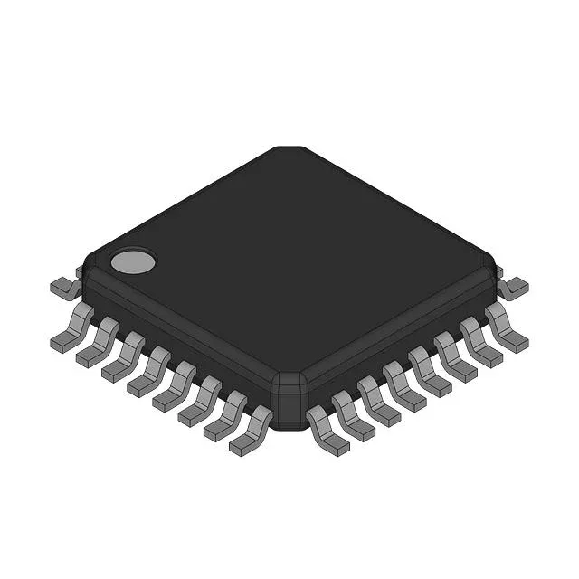
NXP Semiconductors DSP56F802TA80E — Microcontrollers & Processors (MCU / MPU / DSP)

NXP DSP56F802TA80E 16-bit MCU/DSP, 80MHz, 16KB Flash

MPNDSP56F802TA80E
End of Life

NXP Semiconductors 56F8xx series 16-bit MCU/DSP, DSP56F802TA80E, 80MHz core, 16KB Flash, 1K x 16 RAM, 32-LQFP (7x7 mm), -40 to 85°C, ROHS3.

$8.47Ref. price · indicative, final on quote
Packaging32-LQFP
RoHSROHS3 Compliant
Series56F8xx
Sourced new & surplus through independent channelsAuthenticity-screened · ESD-safe packingListing updated Aug 2026

Specifications

DSP56F802TA80E specifications
ParameterValue
Series56F8xx
MountingSurface Mount
Oscillator typeInternal
Program memory typeFLASH
Voltage - supply (Vcc (Vdd))3V ~ 3.6V
Operating temperature-40°C ~ 85°C (TA)
Speed80MHz
PackageBulk
RAM size1K x 16
Core size16-Bit
PeripheralsPOR, PWM, WDT
ConnectivitySCI
Number of i (O)8
Core processor56800
Case32-LQFP
Data convertersA/D 5x12b
Program memory size16KB (8K x 16)

Product details

80 MHz 56800 core — where the DSP meets the MCU

The DSP56F802TA80E is a 16-bit hybrid controller built around the 56800 core — a DSP engine with an MCU control-flow overlay, running at 80 MHz. That clock rate sets the ceiling for the real-time control loop: a sensorless field-oriented current loop on a 10 kHz PWM carrier leaves about 8000 core cycles per interrupt for the observer and PI regulator, which is tight but workable with hand-optimised C or assembly. On-chip memory is 16 KB of flash (8K x 16) and 1K x 16 of RAM — enough for a single motor-control firmware image with a modest data buffer, but not for a communication stack or data-logging overlay. The flash is the program store; the RAM holds the state variables and lookup tables for the control algorithm.

Peripheral set for sensorless motor and power control

The integrated peripherals target exactly the signal chain of a sensorless motor drive: a PWM timer module for three-phase inverter gating, a 5-channel 12-bit ADC for phase current and DC-bus voltage sensing, and a SCI (UART) for commissioning or Modbus RTU pass-through. The POR and WDT handle brown-out and watchdog supervision without an external supervisor IC. The 32-LQFP package (7x7 mm body) keeps the PCB footprint small; the 0.8 mm pitch is routable on a two-layer board with careful trace spacing.

Active lifecycle — where is it in the cycle?

ROHS3 compliant — no exemption expiry to track for EU markets. The part is also REACH and conflict-minerals compliant per NXP's standard declaration, though those documents are not part of this listing.

Frequently asked questions

What is DSP56F802TA80E's closest functional second-source — DSP56F801FA80E?

The DSP56F801FA80E shares the same 80 MHz 56800 core, flash memory size, and peripheral set (POR, PWM, WDT, SCI), but offers 11 I/O (vs 8) and an 8-channel 12-bit ADC (vs 5). The package differs — the FA80E is in a 48-LQFP, not the 32-LQFP of the TA80E. A board respin is required to swap them; they are not pin-compatible.

What compliance documentation does NXP provide for DSP56F802TA80E?

The part is ROHS3 compliant. NXP's standard compliance package includes a ROHS certificate of compliance, REACH declaration, and conflict-minerals reporting. These documents are available from the manufacturer or through the distributor upon request.