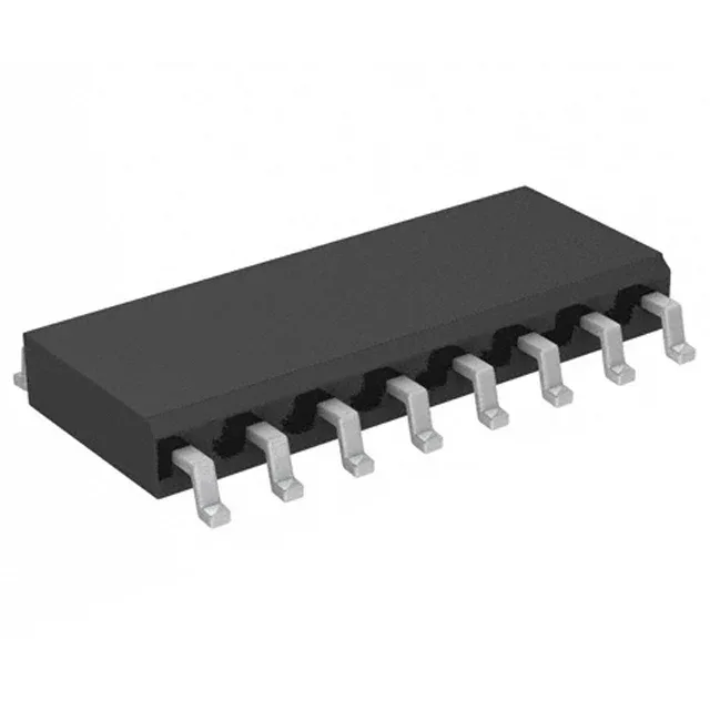
8-bit shift register with a storage register and tri-state bus drive
The NXP 74HCT4094D,112 is an 8-stage shift-and-store register: serial data shifts in on the clock edge, transfers to a parallel storage register on the strobe, and drives the outputs through tri-state buffers. A serial output from the last stage lets you daisy-chain multiple devices for 16, 24, or more bits without external logic. The tri-state outputs (active-low output enable) let multiple registers share a bus; the outputs go high-impedance when OE is high, preventing bus contention in a multiplexed backplane or shared data line.
Temperature grade and package fit for industrial and automotive boards
An ECU or motor-drive controller that sees 105°C on a hot floor still has margin before the part hits its ceiling. Housed in a 16-SOIC narrow-body (3.90 mm width, 1.27 mm pitch), the footprint matches the standard JEDEC SO-16 land pattern. The 16-SO supplier package designation means the same PCB layout works for the SOIC-16 variant from multiple foundries — no board spin if the supply chain shifts.
Because it is an active standard-logic part from the 74HCT family, second-source availability is broad: multiple manufacturers offer pin-compatible 74HCT4094 devices in the same SO-16 package. The BOM is not locked to a single supplier.