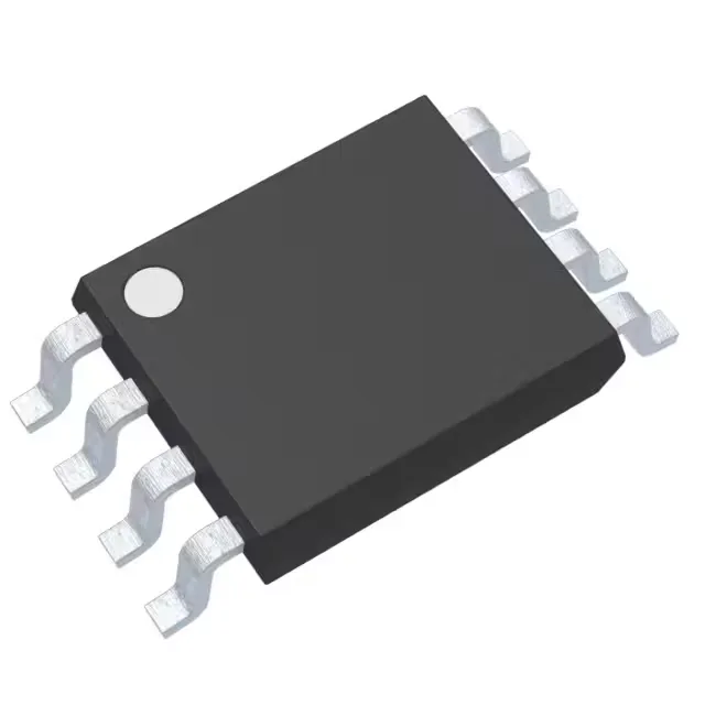
Triple buffer/inverter for ultra-low-power logic
The NXP 74AUP3G0434DC125 is a triple buffer/inverter from the 74AUP series, designed for ultra-low-power and low-voltage logic applications. It operates from a supply voltage range of 0.8 V to 3.6 V, making it suitable for battery-powered and portable devices where power efficiency is critical. With three independent circuits — two inputs on one channel and one input on another — it provides flexible signal buffering or inversion in a single 8-pin package. The single-ended output type simplifies integration into standard logic chains.
Supply voltage and temperature range
The 0.8 V to 3.6 V supply range covers the full low-voltage logic spectrum, from near-threshold operation at 0.8 V up to standard 3.3 V I/O levels. This flexibility allows the part to interface directly with modern low-voltage microcontrollers and FPGAs without level shifting. Rated for -40°C to 125°C operating temperature, it handles industrial and automotive ambient conditions. The wide temperature grade means it can sit in an engine bay or on a rooftop sensor node without derating.
Package and footprint
Housed in an 8-VFSOP package (2.30 mm width, 0.091" body), the 74AUP3G0434DC125 is a surface-mount device with a fine-pitch footprint. The supplier device package is also listed as 8-VSSOP — these are the same physical outline, so the PCB land pattern is interchangeable. The small package suits dense PCB layouts, but hand-soldering is feasible with a fine-tip iron and steady hands — the 0.5 mm pitch leads are visible under a loupe. For rework, a hot-air station at 300°C with a small nozzle works cleanly.
Output drive and logic type
Each output can source or sink 4 mA, which is typical for the AUP family's low-power design. This drive strength is sufficient for driving CMOS logic inputs or low-current LEDs, but not for heavy loads like relays or motors. The part functions as a buffer or inverter — the description lists it as an inverter, but the logic type field says buffer/inverter, so it likely offers both functions depending on the pin configuration. No Schmitt trigger input means the switching threshold follows standard CMOS levels.
Lifecycle and sourcing
Sourced through independent distribution, this part is quoted to order against your BOM quantity. Availability and current pricing are confirmed at RFQ time — no stock-holding claim is made here.