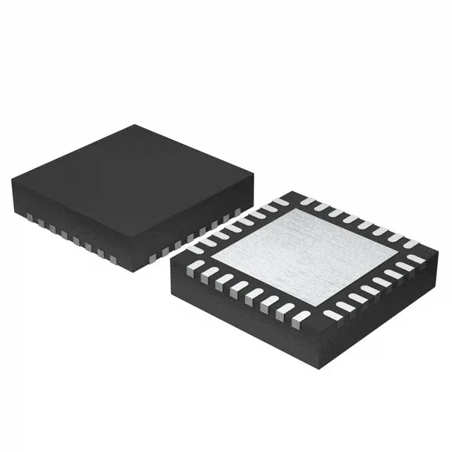
NXP USA Inc. LPC834M101FHI33Y — Microcontrollers & Processors (MCU / MPU / DSP)

NXP LPC834M101FHI33Y ARM Cortex-M0+ MCU, 30 MHz, 32 KB Flash

MPNLPC834M101FHI33Y
Active

NXP LPC83x series 32-bit ARM Cortex-M0+ MCU, LPC834M101FHI33Y, 30 MHz, 32 KB Flash, 4 KB RAM, 12x12b ADC, 29 I/O, 1.8 V–3.6 V supply, -40 °C to 85 °C, 32-HVQFN exposed pad.

$2.6700Ref. price · indicative, final on quote
StockContact for availability
MOQ1 pcs
  • 100% new & originalTraceable channels only — no refurbs, no pulls, no remarked parts.
  • Date & lot codes on quoteStated per line before you commit; label photos on request.
  • MSL-compliant ESD packingMoisture-sealed bags with indicator cards; reels photo-verified.
  • PayPal buyer protectionPay by T/T, PayPal or Payoneer — card payments covered end to end.

Specifications

LPC834M101FHI33Y Technical Specifications
ParameterValue
SeriesLPC83x
Mounting typeSurface Mount
Oscillator typeInternal
Program memory typeFLASH
Voltage - supply (Vcc (Vdd))1.8V ~ 3.6V
Operating temperature-40°C ~ 85°C (TA)
Speed30MHz
PackageTape & Reel (TR) Cut Tape (CT)
RAM size4K x 8
Core size32-Bit Single-Core
PeripheralsBrown-out Detect/Reset, DMA, POR, PWM, WDT
ConnectivityI²C, SPI, UART/USART
Number of i (O)29
Core processorARM® Cortex®-M0+
Case32-VFQFN Exposed Pad
Data convertersA/D 12x12b
Program memory size32KB (32K x 8)

Product details

What this Cortex-M0+ MCU brings to a BOM

The NXP LPC834M101FHI33Y is a 32-bit ARM Cortex-M0+ microcontroller from the LPC83x series, clocked at 30 MHz with 32 KB of Flash and 4 KB of RAM. It integrates a 12-channel 12-bit ADC, 29 general-purpose I/O lines, and serial interfaces (I²C, SPI, UART/USART) in a 32-HVQFN package with an exposed pad for thermal relief. The part operates from a single 1.8 V to 3.6 V supply over the industrial temperature range of -40 °C to 85 °C, making it suitable for sensor hubs, motor-control front-ends, and low-power control nodes in factory automation or outdoor telecom gear.

Memory budget: 32 KB Flash, 4 KB RAM

32 KB of Flash holds a bootloader, a communication protocol, and a state machine. The 4 KB RAM (4K x 8) limits data buffering; use Flash for lookup tables and keep runtime variables lean.

Industrial temperature grade and package

Rated -40 °C to 85 °C, this MCU is qualified for unheated enclosures, engine-bay-adjacent electronics, and outdoor telecom cabinets where condensation and thermal cycling are routine. The 32-HVQFN (5x5 mm) with exposed pad requires a thermal via array under the pad for adequate heat transfer to the ground plane — the datasheet landing pattern is mandatory, not optional. Surface-mount only; no through-hole equivalent exists.

Lifecycle and sourcing posture

The LPC834M101FHI33Y has an Active product status — no last-time-buy notice or obsolescence risk. It is a current-production NXP part available through independent distribution.

Frequently asked questions

What is the operating voltage range of LPC834M101FHI33Y?

The LPC834M101FHI33Y operates from a single 1.8 V to 3.6 V supply, covering both 3.3 V regulated rails and direct Li-ion battery connections without a secondary LDO.

Is LPC834M101FHI33Y pin-compatible with other LPC83x devices?

The LPC834M101FHI33Y shares the same 32-HVQFN footprint and pinout as other LPC83x MCUs in the same package option, allowing memory-density upgrades (e.g., 64 KB Flash variants) without a board respin.

What is the LPC834M101FHI33Y datasheet?

The LPC834M101FHI33Y datasheet is published by NXP under the LPC83x series documentation. It covers the full electrical characteristics, timing diagrams, register map, and application notes for this Cortex-M0+ MCU.