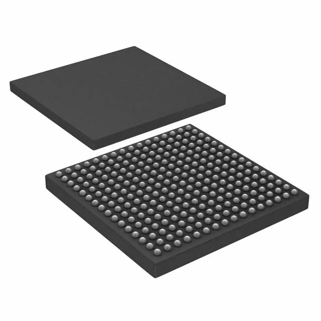
The NXP LPC43S67JET256E pairs an ARM Cortex-M4 running at 204 MHz with a Cortex-M0 companion core, giving you asymmetric multiprocessing in a single 256-LBGA package. The M4 handles DSP, control loops, and the main application stack; the M0 offloads I/O, protocol framing, or housekeeping tasks without stealing M4 cycles. That split saves an external MCU or CPLD on a dense BOM. Program memory is 1 MB Flash, backed by 154 KB SRAM and 16 KB EEPROM — enough headroom for a real-time control stack plus an Ethernet or CANopen fieldbus layer without external memory. The 164 GPIOs cover a large I/O bank, LCD interface, and multiple serial ports simultaneously. Supply range is 2.4 V to 3.6 V. Temperature grade is -40 °C to 105 °C.
Peripherals and connectivity — one-chip gateway
Data converters include a 16-channel 10-bit ADC and a single 10-bit DAC — enough for analog sensor inputs and one analog output, but plan external ADCs if you need higher resolution or more channels.
Lifecycle and sourcing — active, dual-source optional
LPC43xx family includes pin-compatible siblings with different Flash/RAM densities. Base product number LPC43S67 shares the same 256-LBGA footprint.