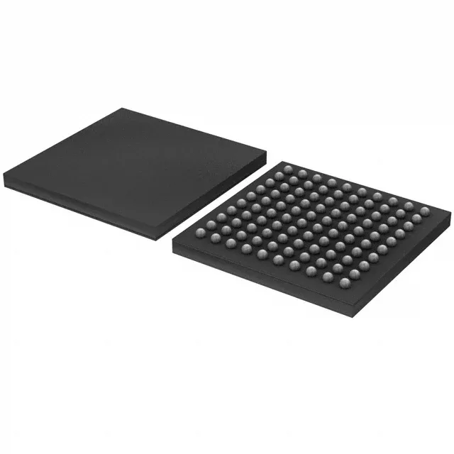
The LPC4315JET100E pairs an ARM Cortex-M4 for DSP and floating-point math with a Cortex-M0 for housekeeping or low-power background tasks, both clocked at 204 MHz. That split lets the M4 handle a motor FOC or audio filter without the M0's interrupt latency jittering the timing. 768 KB of Flash and 136 KB of SRAM give enough room for a modest RTOS stack plus application code; the 16 KB EEPROM block stores calibration constants or boot parameters without wearing the Flash.
Connectivity and peripheral set for industrial control
CANbus, EBI/EMI, I²C, SPI, SSI, SSP, UART/USART, and IrDA cover fieldbus gateways, sensor bridges, and display interfaces. The 4x10-bit ADC and 1x10-bit DAC handle analog feedback loops or simple signal conditioning without an external converter. 49 general-purpose I/O lines are available, though some share functions with the EBI bus — check the pin mux before locking the schematic.
NXP lists the LPC4315JET100E as Active. No last-time-buy or NRND notice is in effect. For dual-sourcing resilience, the LPC43xx family includes pin-compatible density variants; confirm the exact Flash and SRAM requirements before selecting an alternate order code.