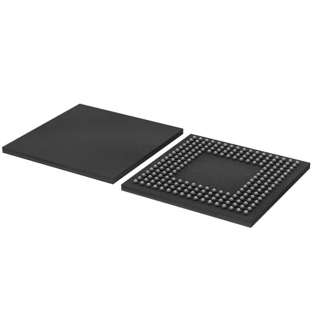
NXP USA Inc. LPC2468FET208,551 — Microcontrollers & Processors (MCU / MPU / DSP)

NXP LPC2468FET208,551 ARM7 MCU, 72MHz, 512KB Flash, 208-TFBGA

MPNLPC2468FET208,551
Active

NXP LPC2400 series ARM7 MCU, LPC2468FET208,551, 16/32-Bit core at 72MHz, 512KB Flash, 98K x 8 RAM, 160 I/O, Ethernet, CAN, USB OTG, 8x10b ADC, 1x10b DAC, -40°C to 85°C, 208-TFBGA (15x15 mm), Tray.

$30.9900Ref. price · indicative, final on quote
StockContact for availability
MOQ1 pcs
  • 100% new & originalTraceable channels only — no refurbs, no pulls, no remarked parts.
  • Date & lot codes on quoteStated per line before you commit; label photos on request.
  • MSL-compliant ESD packingMoisture-sealed bags with indicator cards; reels photo-verified.
  • PayPal buyer protectionPay by T/T, PayPal or Payoneer — card payments covered end to end.

Specifications

LPC2468FET208,551 Technical Specifications
ParameterValue
SeriesLPC2400
Mounting typeSurface Mount
Oscillator typeInternal
Program memory typeFLASH
Voltage - supply (Vcc (Vdd))3V ~ 3.6V
Operating temperature-40°C ~ 85°C (TA)
Speed72MHz
PackageTray
RAM size98K x 8
Core size16/32-Bit
PeripheralsBrown-out Detect/Reset, DMA, I²S, POR, PWM, WDT
ConnectivityCANbus, EBI/EMI, Ethernet, I²C, Microwire, Memory Card, SPI, SSI, SSP, UART/USART, USB OTG
Number of i (O)160
Core processorARM7®
Case208-TFBGA
Data convertersA/D 8x10b; D/A 1x10b
Program memory size512KB (512K x 8)

Product details

72 MHz ARM7 core — processing headroom for protocol stacks

The 72 MHz core clock gives the LPC2468 enough throughput to run a lightweight TCP/IP stack alongside a CANopen or Modbus RTU slave without external protocol co-processors. The 512 KB Flash holds a full firmware image with Ethernet and USB stacks plus application code; the 98K x 8 RAM provides workspace for packet buffers and RTOS task stacks. Designs that need to bridge Ethernet to CAN or drive a local TFT display over the EBI will find the memory partition tight but workable — plan the buffer pool allocation early in the firmware architecture.

208-ball TFBGA — board layout considerations

208-TFBGA package measures 15x15 mm. Routing EBI, Ethernet RMII, and USB differential pairs requires a four-layer PCB minimum.

Active lifecycle — stable for BOM freeze

Active product status per NXP lifecycle classification. No last-time-buy or discontinuation notice issued.

On-chip data converters include an 8-channel 10-bit ADC and a single 10-bit DAC. Internal oscillator eliminates external crystal for non-critical timing.

Frequently asked questions

What is the operating voltage of LPC2468FET208,551?

The supply voltage range is 3.0 V to 3.6 V, allowing operation from a standard 3.3 V rail with 10% tolerance. No separate core voltage is needed.

What is the difference between LPC2468FET208,551 and LPC2478?

The primary difference is that the LPC2478 integrates an LCD controller for direct TFT panel driving, while the LPC2468 does not. Both share the same ARM7 core, 72 MHz clock, 512 KB Flash, 98K x 8 RAM, and peripheral set (Ethernet, CAN, USB OTG). If your design requires a local display, the LPC2478 saves an external graphics controller; otherwise the LPC2468 is functionally equivalent at a lower BOM cost.

What is the pinout diagram for LPC2468FET208,551?

The pinout diagram is provided in the NXP LPC2468 datasheet, which maps the 208-ball TFBGA ball assignments. The base product number is LPC2468; the full datasheet covers ball-out, electrical characteristics, and application information.