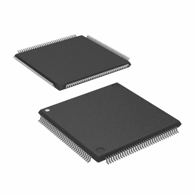
The NXP LPC2210FBD144/01K is a 16/32-bit ARM7 MCU clocked at 75 MHz. It's a ROMless device — no internal Flash — so the firmware lives on an external SPI or parallel NOR Flash, accessed through the External Bus Interface (EBI/EMI). On-chip resources include 16 KB SRAM (organized as 16K x 8), 76 GPIO lines, an 8-channel 10-bit ADC, and a full set of serial interfaces: I²C, SPI, Microwire, SSI, SSP, and UART/USART.
ROMless architecture — plan the external memory early
Because there's no on-chip program memory, the boot sequence must fetch the first instruction from an external device. Typical setups use a parallel NOR Flash on the EBI (16-bit wide for best throughput) or a serial SPI Flash with a small bootloader in the 16 KB SRAM. The 16 KB SRAM is enough for stack and moderate data buffers, but complex control algorithms or TCP/IP stacks will need external SRAM or SDRAM on the EBI. The ADC's 10-bit resolution and 8 channels suit analog sensor inputs for temperature, pressure, or current monitoring in industrial I/O modules.
If you're dual-sourcing, NXP's LPC2200 family includes pin-compatible siblings with varying SRAM and peripheral sets — check the specific memory map and ADC channel count against your firmware before swapping. The 144-LQFP footprint is common across the series, so a board spin for a different density is usually a firmware-only change.