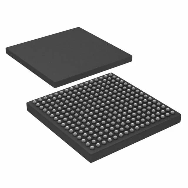
NXP USA Inc. LPC1857JET256,551 — Microcontrollers & Processors (MCU / MPU / DSP)

NXP LPC1857JET256,551 ARM Cortex-M3 MCU, 180 MHz, 1 MB Flash, 256-LBGA

MPNLPC1857JET256,551
Active

NXP LPC18xx series, 32-bit ARM Cortex-M3 MCU, LPC1857JET256,551, 180 MHz, 1 MB Flash, 136 KB SRAM, 16 KB EEPROM, 164 I/O, Ethernet, CAN, USB OTG, 2.2 V to 3.6 V, -40 to 105 °C, 256-LBGA (17x17 mm).

$21.9400Ref. price · indicative, final on quote
StockContact for availability
MOQ1 pcs
  • 100% new & originalTraceable channels only — no refurbs, no pulls, no remarked parts.
  • Date & lot codes on quoteStated per line before you commit; label photos on request.
  • MSL-compliant ESD packingMoisture-sealed bags with indicator cards; reels photo-verified.
  • PayPal buyer protectionPay by T/T, PayPal or Payoneer — card payments covered end to end.

Specifications

LPC1857JET256,551 Technical Specifications
ParameterValue
SeriesLPC18xx
Mounting typeSurface Mount
Oscillator typeInternal
Program memory typeFLASH
Voltage - supply (Vcc (Vdd))2.2V ~ 3.6V
Operating temperature-40°C ~ 105°C (TA)
Speed180MHz
PackageTray
RAM size136K x 8
Core size32-Bit Single-Core
EEPROM size16K x 8
PeripheralsBrown-out Detect/Reset, DMA, I²S, LCD, Motor Control PWM, POR, PWM, WDT
ConnectivityCANbus, EBI/EMI, Ethernet, I²C, IrDA, Microwire, QEI, SD, SPI, SSI, SSP, UART/USART, USB, USB OTG
Number of i (O)164
Core processorARM® Cortex®-M3
Case256-LBGA
Data convertersA/D 8x10b; D/A 1x10b
Program memory size1MB (1M x 8)

Product details

180 MHz Cortex-M3 — throughput for protocol stacks and control loops

The 180 MHz core clock is the highest speed grade in the LPC18xx Cortex-M3 line. At this frequency, the MCU can run a full Ethernet TCP/IP stack, a CANopen master, and a motor-control loop without saturating the CPU. The 136 KB SRAM provides enough working memory for dual Ethernet packet buffers (typically 16–32 KB each) and an RTOS heap, reducing the need for external SRAM in many designs.

On-chip EEPROM and data converters

16 KB of EEPROM is available for calibration constants, configuration parameters, or fail-safe boot settings without wearing the main Flash. The analog subsystem includes an 8-channel 10-bit ADC and a single 10-bit DAC, sufficient for monitoring motor currents or setting an analog reference in a control loop.

Lifecycle and sourcing posture

NXP lists the part as Active — no last-time-buy or end-of-life notice is in effect. Sourced and quoted to order through independent distribution.

Frequently asked questions

What is the operating temperature range of LPC1857JET256?

The operating temperature range is -40 to 105 °C, qualifying it for industrial and automotive under-hood environments.

What is the operating voltage of LPC1857JET256?

The supply voltage range is 2.2 V to 3.6 V, compatible with standard 3.3 V and 2.5 V system rails.

Does LPC1857JET256 have I2C interfaces?

Yes, the connectivity set includes I²C interfaces, along with SPI, UART, SSI, SSP, IrDA, and Microwire.

Are there equivalents to LPC1857JET256?

Pin-compatible alternatives exist within the LPC18xx family at lower Flash or SRAM densities; the LPC1857JET256 is the highest-density variant in the series. No official second-source alternate is listed by NXP.