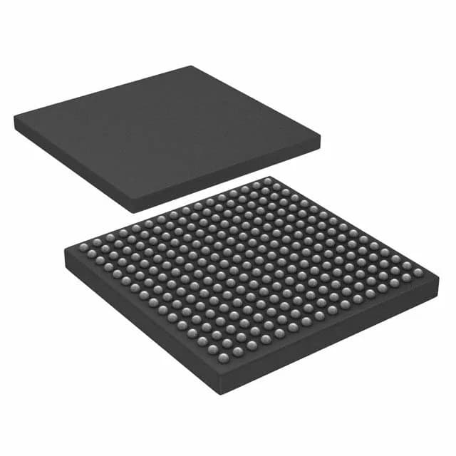
NXP USA Inc. LPC1857FET256,551 — Microcontrollers & Processors (MCU / MPU / DSP)

NXP LPC1857FET256,551 ARM Cortex-M3 MCU, 180 MHz, 1 MB Flash, 256-LBGA

MPNLPC1857FET256,551
Active

NXP LPC18xx series 32-bit ARM Cortex-M3 MCU, LPC1857FET256,551, 180 MHz, 1 MB Flash, 136 KB RAM, Ethernet, CAN, USB OTG, 164 I/O, 256-LBGA, -40°C to 85°C.

$21.7700Ref. price · indicative, final on quote
StockContact for availability
MOQ1 pcs
  • 100% new & originalTraceable channels only — no refurbs, no pulls, no remarked parts.
  • Date & lot codes on quoteStated per line before you commit; label photos on request.
  • MSL-compliant ESD packingMoisture-sealed bags with indicator cards; reels photo-verified.
  • PayPal buyer protectionPay by T/T, PayPal or Payoneer — card payments covered end to end.

Specifications

LPC1857FET256,551 Technical Specifications
ParameterValue
SeriesLPC18xx
Mounting typeSurface Mount
Oscillator typeInternal
Program memory typeFLASH
Voltage - supply (Vcc (Vdd))2.2V ~ 3.6V
Operating temperature-40°C ~ 85°C (TA)
Speed180MHz
PackageTray
RAM size136K x 8
Core size32-Bit Single-Core
EEPROM size16K x 8
PeripheralsBrown-out Detect/Reset, DMA, I²S, LCD, Motor Control PWM, POR, PWM, WDT
ConnectivityCANbus, EBI/EMI, Ethernet, I²C, IrDA, Microwire, QEI, SD, SPI, SSI, SSP, UART/USART, USB, USB OTG
Number of i (O)164
Core processorARM® Cortex®-M3
Case256-LBGA
Data convertersA/D 8x10b; D/A 1x10b
Program memory size1MB (1M x 8)

Product details

180 MHz Cortex-M3 — what the speed buys you

The 180 MHz core is the fastest clock available in the LPC18xx series. It directly determines how much headroom you have for real-time control loops, TCP/IP stack processing, or display refresh. At this speed, a single-cycle multiply or a 16-bit timer capture runs without stalling the CPU — useful when the part is handling both a CANopen stack and a PWM motor-control interrupt simultaneously.

Memory sizing: 1 MB Flash, 136 KB RAM, 16 KB EEPROM

The 1 MB Flash is enough for a dual-image firmware layout (bootloader + application) with room for a small file system. The 136 KB SRAM is split across multiple banks; it can hold a 640x480 frame buffer at 16-bit colour if you use the external bus for the display controller. The 16 KB EEPROM emulation area is useful for storing calibration constants or configuration parameters that survive a firmware update.

Lifecycle and sourcing status

The LPC1857FET256,551 is listed as Active in production. No last-time-buy or end-of-life notice has been issued. For current pricing and availability, the part is sourced and quoted to order through independent distribution — submit an RFQ for a confirmed quote and lead time at the time of order.

Temperature grade and environment

Rated for -40°C to 85°C ambient, this part suits factory automation and outdoor telecom cabinets. The 256-LBGA package is surface-mount only.

Frequently asked questions

Where can I find the LPC1857FET256 datasheet?

The datasheet for the LPC1857FET256,551 is available from NXP's official documentation portal. The base product number is LPC1857.

What is the LPC1857FET256,551's core speed?

The LPC1857FET256,551 runs at 180 MHz on a 32-bit ARM Cortex-M3 core.

What tools and programmers support the LPC1857FET256,551?

The LPC1857FET256,551 is supported by standard ARM Cortex-M debug tools including J-Link, ULINK, and CMSIS-DAP probes. NXP's MCUXpresso IDE and SDK provide full peripheral driver support for the LPC18xx series.