What this MCU brings to the BOM
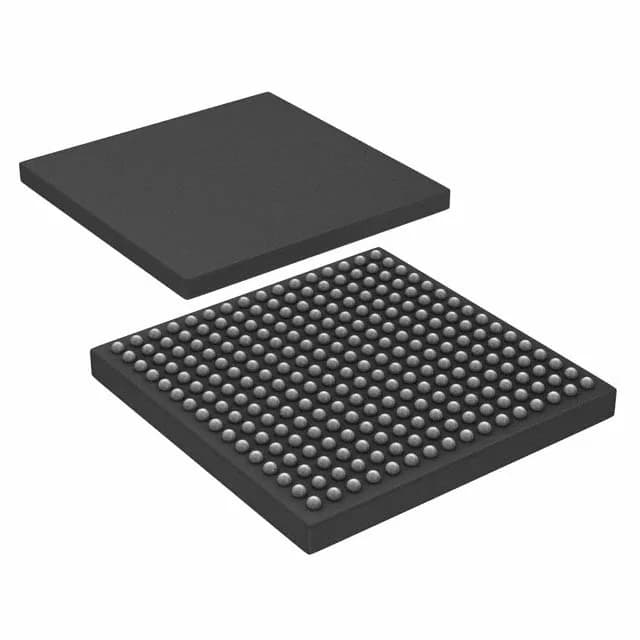
The NXP LPC1837FET256,551 is a 32-bit ARM Cortex-M3 microcontroller running at 150 MHz, with 1 MB of on-chip Flash and 136K x 8 of SRAM. It targets industrial control, motor-drive, and communication-gateway applications where a single-chip MCU must handle both real-time loops and protocol stacks like Ethernet, CAN, and USB OTG without an external host processor. The 80 general-purpose I/O lines and the internal oscillator keep the external BOM lean — no crystal needed for basic operation, and the 256-LBGA (17x17 mm) package fits a four-layer board without heroic routing. Supply range of 2 V to 3.6 V.
150 MHz Cortex-M3 — what it means for throughput
At 150 MHz the Cortex-M3 delivers 150 MHz clock speed. The DMA engine offloads peripheral transfers.
Memory sizing and field-update reality
1 MB of Flash holds a full firmware image plus a fallback bootloader for over-the-air or fieldbus-driven updates. The 136K x 8 SRAM leaves room for a TCP/IP buffer pool and a few kilobytes of real-time data without needing external RAM. If your application needs more than 136 KB of working memory, plan for an external SDRAM or SRAM on the EBI/EMI bus — the LPC1837 supports that directly.
Connectivity and peripheral set
The part integrates CAN, Ethernet, USB OTG, multiple I²C and SPI/SSP ports, plus a Motor Control PWM block with dead-time insertion. That means one MCU can act as a fieldbus gateway, a servo drive controller, and a data-logging node. The 16-channel 10-bit ADC and single 10-bit DAC handle analog feedback from current sensors or potentiometers.
Temperature grade and environment
Rated for -40°C to 85°C ambient. The 256-LBGA package is a standard ball-grid array.
Lifecycle and sourcing posture
The LPC1837FET256,551 carries an Active lifecycle status from NXP. No last-time-buy or EOL notice is on record. For BOM-freeze planning, this part is a safe choice for new designs and long-run production. Sourced and quoted to order against an RFQ through independent distribution; availability and current pricing confirmed at quote time.