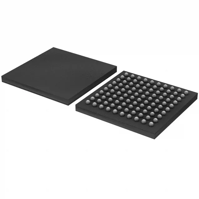
NXP USA Inc. LPC1825JET100E — Microcontrollers & Processors (MCU / MPU / DSP)

NXP LPC1825JET100E ARM Cortex-M3 MCU, 180MHz, 768KB Flash, 136KB SRAM

MPNLPC1825JET100E
Active

NXP LPC18xx series ARM Cortex-M3 32-bit single-core MCU, LPC1825JET100E, 180MHz, 768KB Flash, 136KB SRAM, 16KB EEPROM, 49 I/O, CAN, USB OTG, 4×10b ADC, 1×10b DAC, 2.2–3.6V supply, -40°C to 105°C, 100-TFBGA (9×9) tray.

$13.4640Ref. price · indicative, final on quote
StockContact for availability
MOQ1 pcs
  • 100% new & originalTraceable channels only — no refurbs, no pulls, no remarked parts.
  • Date & lot codes on quoteStated per line before you commit; label photos on request.
  • MSL-compliant ESD packingMoisture-sealed bags with indicator cards; reels photo-verified.
  • PayPal buyer protectionPay by T/T, PayPal or Payoneer — card payments covered end to end.

Specifications

LPC1825JET100E Technical Specifications
ParameterValue
SeriesLPC18xx
Mounting typeSurface Mount
Oscillator typeInternal
Program memory typeFLASH
Voltage - supply (Vcc (Vdd))2.2V ~ 3.6V
Operating temperature-40°C~105°C(TA)
Speed180MHz
PackageTray
RAM size136K x 8
Core size32-Bit Single-Core
EEPROM size16K x 8
PeripheralsBrown-out Detect/Reset, DMA, I²S, POR, WDT
ConnectivityCANbus, EBI/EMI, I²C, IrDA, Microwire, SD, SPI, SSI, SSP, UART/USART, USB, USB OTG
Number of i (O)49
Core processorARM® Cortex®-M3
Case100-TFBGA
Data convertersA/D 4x10b; D/A 1x10b
Program memory size768KB (768K x 8)

Product details

180 MHz Cortex-M3 — what it means for the control loop

The NXP LPC1825JET100E is a 32-bit ARM Cortex-M3 single-core MCU running at 180 MHz, with 768 KB of Flash program memory and 136 KB of SRAM. It carries 16 KB of EEPROM for parameter storage, 49 general-purpose I/O lines, and a rich peripheral set including CANbus, USB OTG, an external bus interface (EBI/EMI), multiple SPI/I²C/UART serial ports, and I²S audio. On-chip data converters provide a 4-channel 10-bit ADC and a single 10-bit DAC. The part operates from 2.2 V to 3.6 V and is rated over the industrial temperature range of -40°C to 105°C, making it suitable for factory automation, motor control, industrial communication gateways, and outdoor telecom equipment where extended temperature tolerance is required.

768 KB Flash and 136 KB SRAM — sizing the firmware and data buffers

The 768 KB Flash is a mid-range density within the LPC18xx family — enough for a full communication stack (TCP/IP, CANopen, USB device) plus application logic, without needing external memory for code. The 136 KB SRAM supports moderate data buffering, multitasking with a real-time OS, and DMA transfers. If your application requires larger data arrays or frame buffers, the external memory interface (EBI/EMI) on this package variant provides a path to add SRAM or Flash externally.

Connectivity and peripherals — CAN, USB OTG, EBI/EMI

The LPC1825JET100E integrates CANbus for industrial networking, USB OTG for dual-role device/host connectivity, and an external bus interface (EBI/EMI) for parallel memory or FPGA attachment. The 49 I/O lines are multiplexed with these peripherals; pin assignment planning is essential to avoid conflicts. The 100-TFBGA (9x9 mm) package requires a multi-layer PCB with micro-vias or fine-pitch routing for the BGA balls — not a hand-wire prototype part. The internal oscillator eliminates the need for an external crystal in many applications, though an external clock source can be used for tighter timing accuracy.

Frequently asked questions

What is LPC1825JET100E's listed speed?

The LPC1825JET100E runs at 180 MHz, which is the maximum core clock for this ARM Cortex-M3 device.