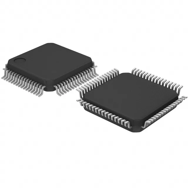
NXP USA Inc. LPC1549JBD64QL — Microcontrollers & Processors (MCU / MPU / DSP)

NXP LPC1549JBD64QL ARM Cortex-M3 MCU, 72 MHz, 256 KB Flash, 64-LQFP

MPNLPC1549JBD64QL
Active

NXP LPC15xx series, ARM Cortex-M3 32-bit MCU, 256KB Flash / 36KB RAM, 72MHz clock, 24-channel 12-bit ADC, CANbus and USB on-chip, 44 I/O, 2.4–3.6 V supply, 64-LQFP (10×10 mm), tray, -40°C to 105°C.

$13.7000Ref. price · indicative, final on quote
Packaging64-LQFP
RoHSROHS3 Compliant
SeriesLPC15xx
Independent supplier — new & surplus stockAuthenticity-screened · ESD-safe packingListing updated Jul 2026

Specifications

LPC1549JBD64QL specifications
ParameterValue
SeriesLPC15xx
MountingSurface Mount
Oscillator typeInternal
Program memory typeFLASH
Voltage - supply (Vcc (Vdd))2.4V ~ 3.6V
Operating temperature-40°C ~ 105°C (TA)
Speed72MHz
PackageTray
RAM size36K x 8
Core size32-Bit Single-Core
EEPROM size4K x 8
PeripheralsBrown-out Detect/Reset, DMA, POR, PWM, WDT
ConnectivityCANbus, I²C, SPI, UART/USART, USB
Number of i (O)44
Core processorARM® Cortex®-M3
Case64-LQFP
Data convertersA/D 24x12b
Program memory size256KB (256K x 8)

Product details

72 MHz Cortex-M3 — throughput for control loops

The LPC1549JBD64QL: The 72 MHz core clock on the ARM Cortex-M3 gives this MCU enough headroom to run a real-time control loop (e.g., a field-oriented motor control algorithm) alongside a CANbus stack without stalling. The 36 KB RAM handles moderate data buffers for sensor fusion or communication packets; if your application needs larger frame buffers, the 256 KB Flash can also store lookup tables executed in place.

24-channel ADC — analog front-end integration

On-chip CAN and USB — reduced external IC count

CANbus and USB controllers are built into the silicon, so you only need a physical-layer transceiver to connect to a fieldbus or host port. This integration cuts component count and simplifies PCB layout for industrial gateways, programmable logic controllers, and embedded human-machine interfaces.

It is ROHS3 compliant. No end-of-life notice is recorded.

Frequently asked questions

What is the pinout and supply voltage for LPC1549JBD64QL?

The LPC1549JBD64QL operates from a 2.4 V to 3.6 V supply and is available in a 64-LQFP (10×10 mm) package. The full pinout is in the NXP LPC15xx datasheet.

What is the difference between LPC1549 and LPC1548?

The LPC1549JBD64QL offers 256 KB Flash and 36 KB RAM, while the LPC1548 typically has 128 KB Flash and 20 KB RAM. Both are pin-compatible in the same 64-LQFP package, so the LPC1549 is the higher-density option for firmware growth.

Is LPC1549JBD64QL compatible with 3.3 V logic?

Yes, the 2.4 V to 3.6 V supply range includes 3.3 V, and all I/O pins are 3.3 V tolerant. No level shifters are needed for standard 3.3 V peripherals.

Where can I buy LPC1549JBD64QL?

The LPC1549JBD64QL is available to order through independent distribution. Submit an RFQ for current availability and pricing — stock levels and lead times are confirmed at quote time.