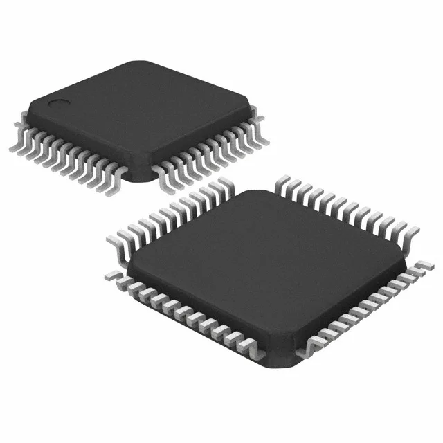
NXP USA Inc. LPC11U12FBD48/201, — Microcontrollers & Processors (MCU / MPU / DSP)

LPC11U12FBD48/201, NXP LPC11U12FBD48/201 ARM Cortex-M0 MCU, 50 MHz, 16 KB Flash,

MPNLPC11U12FBD48/201,
Active

NXP LPC11Uxx series 32-bit ARM Cortex-M0 MCU, 50 MHz, 16 KB Flash, 6 KB SRAM, USB 2.0 device, 40 I/O, 8-channel 10-bit ADC, 1.8 V to 3.6 V supply, -40 to 85 °C, 48-LQFP package, Tray.

$4.7700Ref. price · indicative, final on quote
Packaging48-LQFP
RoHSROHS3 Compliant
SeriesLPC11Uxx
Sourced new & surplus through independent channelsAuthenticity-screened · ESD-safe packingListing updated Jul 2026

Specifications

LPC11U12FBD48/201, specifications
ParameterValue
SeriesLPC11Uxx
MountingSurface Mount
Oscillator typeInternal
Program memory typeFLASH
Voltage - supply (Vcc (Vdd))1.8V ~ 3.6V
Operating temperature-40°C ~ 85°C (TA)
Speed50MHz
PackageTray
RAM size6K x 8
Core size32-Bit Single-Core
PeripheralsBrown-out Detect/Reset, POR, WDT
ConnectivityI²C, Microwire, SmartCard, SPI, SSP, UART/USART, USB
Number of i (O)40
Core processorARM® Cortex®-M0
Case48-LQFP
Data convertersA/D 8x10b
Program memory size16KB (16K x 8)

Product details

50 MHz Cortex-M0 — enough headroom for USB and protocol handling

The LPC11U12FBD48/201,: The 50 MHz core speed on the Cortex-M0 gives you roughly 50 MIPS of single-cycle integer throughput. That is enough to run a USB CDC/ACM virtual COM port at full speed without external PHY, while leaving cycles for polling the ADC or servicing a SPI flash.

USB connectivity and serial interfaces

The USB full-speed device controller supports control, bulk, interrupt, and isochronous transfers.

Memory sizing — what fits in 16 KB Flash and 6 KB SRAM

16 KB of Flash is enough for a USB HID class driver, a bootloader, and application logic for a simple sensor node or a keypad controller. The 6 KB SRAM handles USB endpoint buffers plus a modest data stack.

Frequently asked questions

What is the operating voltage range of LPC11U12FBD48/201?

The supply voltage range is 1.8 V to 3.6 V, which covers both 1.8 V and 3.3 V logic systems. It is compatible with 3.3 V logic without level shifting.

What is the pinout of LPC11U12FBD48/201?

The part is supplied in a 48-LQFP package (7x7 mm body) with 40 general-purpose I/O pins. The pinout follows the standard LPC11Uxx 48-pin layout, which is shared across the family for density upgrades.

What is the equivalent or replacement for LPC11U12FBD48/201?

Within the LPC11Uxx series, the LPC11U14 and LPC11U24 are pin-compatible upgrades offering 32 KB and 64 KB Flash respectively, with the same 48-LQFP footprint. No direct second-source alternate from another manufacturer is listed in the official cross-reference.