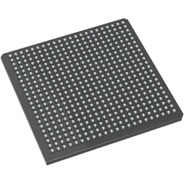
Microchip Technology M2S005-FGG484I — Memory (DRAM / SRAM / Flash / EEPROM)

M2S005-FGG484I SmartFusion2 SoC FPGA, 166MHz, 484-FPBGA

MPNM2S005-FGG484I
End of Life

Microchip SmartFusion®2 M2S005-FGG484I SoC FPGA, ARM® Cortex®-M3 core at 166MHz, 128KB Flash, 64KB RAM, 5K logic modules, 209 I/O, DDR, CAN/Ethernet/USB, 484-FPBGA (23x23), -40°C to 100°C, Tray.

$26.91Ref. price · indicative, final on quote
Packaging484-BGA
StockContact for availability
MOQ1 pcs
  • 100% new & originalTraceable channels only — no refurbs, no pulls, no remarked parts.
  • Date & lot codes on quoteStated per line before you commit; label photos on request.
  • MSL-compliant ESD packingMoisture-sealed bags with indicator cards; reels photo-verified.
  • PayPal buyer protectionPay by T/T, PayPal or Payoneer — card payments covered end to end.

Specifications

M2S005-FGG484I Technical Specifications
ParameterValue
SeriesSmartFusion®2
Operating temperature-40°C ~ 100°C (TJ)
Speed166MHz
PackageTray
RAM size64KB
Flash size128KB
PeripheralsDDR
ArchitectureMCU, FPGA
ConnectivityCANbus, Ethernet, I²C, SPI, UART/USART, USB
Number of i (O)209
Core processorARM® Cortex®-M3
Case484-BGA
Primary attributesFPGA - 5K Logic Modules

Product details

166 MHz Cortex-M3 with 5K logic modules — what this buys the design

The Microchip M2S005-FGG484I is a SmartFusion®2 SoC FPGA that integrates an ARM® Cortex®-M3 processor core running at 166 MHz with 5K logic modules of FPGA fabric on a single die. This architecture lets you offload deterministic real-time control loops or custom peripheral logic into the programmable logic while the hard processor handles communications and higher-level firmware. The 128 KB of embedded Flash and 64 KB of SRAM are sized for moderate firmware images and runtime data; if your application needs more memory headroom, the DDR peripheral interface allows external SDRAM expansion.

The 484-FPBGA package (23x23 mm body) requires a multilayer PCB with at least four signal layers for fanout of the 209 I/O; Microchip's layout guidelines recommend a 0.8 mm pitch with 0.35 mm via pad diameter for reliable routing.

Connectivity and peripherals — what is on-chip

This peripheral set covers the common industrial communication buses — CAN for motor drives, Ethernet for SCADA links, and USB for configuration or data logging. The FPGA fabric can implement additional serial interfaces (e.g., custom SPI masters, PWM generators, quadrature encoder decoders) using the 5K logic modules, which is roughly equivalent to a small CoolRunner-II or MAX V CPLD in gate count.

This is a standard product within the SmartFusion®2 family, so supply should remain stable through the typical 10–15 year lifecycle of industrial designs. The part is ROHS3 compliant, which simplifies EU and global regulatory acceptance.

Frequently asked questions

What is the difference between M2S005-FGG484I and M2S005-FGG484?

The 'I' version is the correct choice for environments where ambient temperatures exceed 70°C or where the junction may reach 100°C under full load.

What are the programming tools for M2S005-FGG484I?

Microchip's Libero® SoC Design Suite supports the SmartFusion®2 family, including the M2S005-FGG484I. It provides the FPGA synthesis, place-and-route, and the embedded software development environment for the Cortex-M3 core. Programming is done via the JTAG interface using a FlashPro5 programmer or compatible third-party tools.