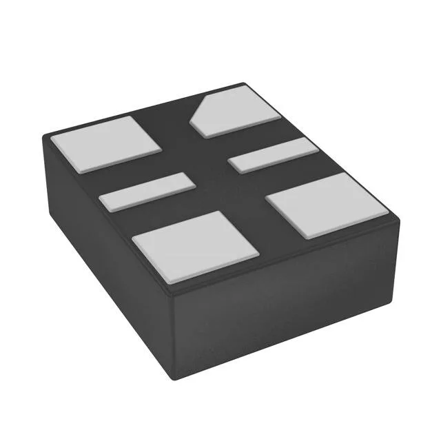
94 MHz LVDS clock source with MEMS resonator
The LVDS output delivers the differential swing needed for high-speed clock distribution to FPGAs, SerDes, and gigabit transceivers without the common-mode noise coupling that single-ended clocks pick up on long traces.
Supply voltage flexibility and package footprint
The supply voltage range spans 2.5V to 3.3V, so the same order code works in a 2.5V FPGA bank or a 3.3V clock fanout buffer without a separate regulator. The 6-VDFN package measures 5.00 mm x 3.20 mm with a seated height of 0.90 mm — a low-profile footprint that fits tight mezzanine card stacks and single-board computers.