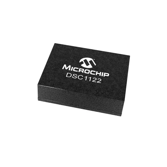
Microchip Technology DSC1224BL2-100M0000T — Crystals & Oscillators

DSC1224BL2-100M0000T 100 MHz HCSL MEMS Oscillator

MPNDSC1224BL2-100M0000T
Active

Microchip DSC1224BL2-100M0000T, XO (Standard) MEMS oscillator, 100 MHz HCSL output, ±25 ppm stability, -40°C to 105°C, 2.5V to 3.3V supply, 6-VDFN package

Sourced new & surplus through independent channelsAuthenticity-screened · ESD-safe packingListing updated Aug 2026

Specifications

DSC1224BL2-100M0000T specifications
ParameterValue
TypeXO (Standard)
SeriesDSC1224
MountingSurface Mount
Voltage2.5V ~ 3.3V
Current - supply40mA (Typ)
Current - supply (Disable)23mA (Typ)
Frequency100 MHz
Frequency stability±25ppm
Operating temperature-40°C~105°C
Size (Dimension)0.197\" L x 0.126\" W (5.00mm x 3.20mm)
Height - seated0.035\" (0.90mm)
OutputHCSL
PackageTape & Reel (TR)
FunctionEnable/Disable
Base resonatorMEMS
Case6-VDFN

Product details

100 MHz HCSL reference clock for PCIe and high-speed interfaces

The DSC1224BL2-100M0000T is a 100 MHz MEMS-based XO with HCSL output, designed to serve as a reference clock for PCIe Gen1/2/3, Ethernet, and FPGA transceiver blocks. The HCSL (High-Speed Current Steering Logic) output provides the differential swing and common-mode levels required by PCIe without external termination resistors — the receiver's 50 Ω to ground on each leg sets the bias.

Supply flexibility and enable/disable control

The 2.5V to 3.3V supply range lets the same part serve 2.5V and 3.3V logic domains — no separate voltage variant or external LDO needed when moving between FPGA banks or switching to a lower-voltage SoC.

Frequently asked questions

What is the HCSL output compatibility of DSC1224BL2-100M0000T?

The HCSL output is directly compatible with PCIe reference clock inputs (PCIe Gen1/2/3) and many FPGA transceiver reference clock pins. The differential swing and common-mode levels meet the PCIe Base Spec without external bias resistors — the receiver's 50 Ω to ground on each leg sets the proper termination.

What voltage supply does DSC1224BL2-100M0000T require?

The oscillator operates from a 2.5V to 3.3V supply, covering both common logic rails. The same part can be used in a 2.5V FPGA bank or a 3.3V SoC reference clock without a separate voltage variant.

What is the frequency stability of DSC1224BL2-100M0000T?

This is tight enough for PCIe reference clock jitter budgets without a TCXO.