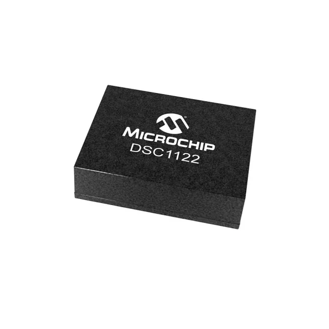
125 MHz LVDS clock with MEMS resonator
Output is LVDS, the differential signalling standard that keeps the clock edge clean across a PCB trace up to several inches — the 125 MHz fundamental lands at the receiver with controlled impedance and minimal radiated EMI.
For a 125 MHz carrier, ±20 ppm equals ±2.5 kHz of absolute frequency error, well within the capture range of most SERDES PLLs. The wide supply range of 2.5V to 3.3V means the same oscillator can be shared across a 2.5V FPGA bank and a 3.3V Ethernet PHY without a dedicated regulator — the internal LDO on the MEMS die absorbs the rail variation.
Standby mode draws 5 µA
Wake-up time from standby is typically under 10 ms, fast enough for duty-cycled IoT gateways or sensor nodes that sleep between data bursts. Active current is 32 mA typ at 125 MHz — the LVDS output stage drives 100-ohm terminated lines with a 350 mV swing; the current is dominated by the output buffer, not the MEMS core.
Housed in a 6-VDFN package measuring 7.00 mm × 5.00 mm with a seated height of 0.90 mm — the low profile fits under a heatsink or behind a display bezel.