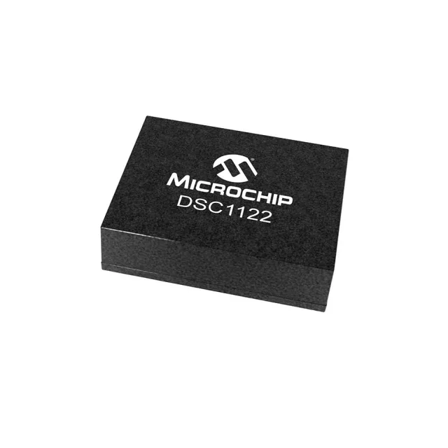
125 MHz LVDS clock for industrial timing trees
The DSC1203CI3-125M0000T: LVDS differential signalling keeps the 125 MHz edge clean over short PCB traces — the 32 mA typical supply current is the power budget for the oscillator alone, not the termination resistors. The MEMS base resonator means no quartz crystal aging curve to track, but the phase-noise floor is higher than a quartz-based VCXO at the same frequency — fine for Ethernet and FPGA reference clocks, less suited to RF synthesis.
Supply voltage range is 2.5 V to 3.3 V, so the same BOM line can serve a 2.5 V FPGA bank or a 3.3 V PHY without a separate regulator.
Housed in a 6-VDFN package measuring 3.20 mm x 2.50 mm with a seated height of 0.90 mm — the small footprint leaves room for decoupling caps close to the supply pin, which is critical for LVDS signal integrity at 125 MHz.