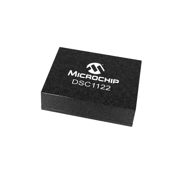
270 MHz LVDS clock source with MEMS ruggedness
The LVDS differential pair keeps the 270 MHz edge clean over a few inches of trace, which is why you see this part in high-speed SerDes reference clocks or FPGA transceiver banks. Supply voltage range is 2.5V to 3.3V, so it drops into either a 2.5V or 3.3V clock domain without a separate regulator.
Industrial temperature and standby power
The 6-VDFN package (5.0 mm × 3.2 mm) is a standard footprint — rework is straightforward with hot air if you preheat the board to 100°C first to avoid lifting the pad. Active current is 32 mA typical, and the standby (power-down) pin drops draw to 5 µA max. That standby mode lets a microcontroller or FPGA gate the clock off when the high-speed bus is idle, saving power in battery-backed or thermally constrained designs.