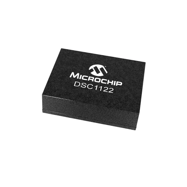
The LVDS output delivers the differential signaling needed for FPGA reference clocks, SerDes reference inputs, and high-speed ADC/DAC clocking — the 200 MHz carrier supports data rates up to 400 Mbps in double-data-rate links.
Supply voltage tolerance and power-down capability
Supply voltage spans 2.5V to 3.3V, so the same order code works on a 2.5V FPGA bank or a 3.3V clock fan-out buffer — no separate voltage-grade variant to manage on the BOM.
MEMS resonator advantage in mechanical environments
Product status is Active.