125K-gate ProASIC3 — what the density buys you
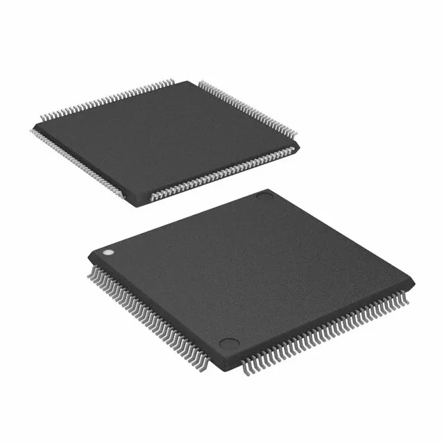
The Microchip A3P125-TQG144 is a ProASIC3 family FPGA with 125000 system gates, 100 user I/O, and 36864 bits of embedded SRAM in a 144-pin LQFP package. This is a flash-based, single-chip FPGA — no external configuration memory needed, instant-on at power-up. The 125K gate count places it in the mid-range of the ProASIC3 family, suitable for glue-logic consolidation, bus bridging, or control-plane sequencing in industrial and commercial equipment. The 100 I/O are available in the 144-LQFP package, giving good pin-to-gate ratio for designs that need parallel interfaces or many discrete signals.
Supply rail — why the 1.5V tolerance matters
The core supply range is 1.425V to 1.575V — a tight ±50 mV window around 1.5V. The board needs a dedicated 1.5V rail with ±3% regulation or better; a generic adjustable LDO set to 1.5V with 1% feedback resistors works, but the regulator must handle the FPGA's inrush without drooping below 1.425V. The I/O banks are powered separately (not specified in this listing, but typical ProASIC3 parts use 3.3V or 2.5V VCCI) — check the full datasheet for bank voltage assignments before laying out the PCB.
Temperature grade — controlled environment only
This is a commercial/industrial indoor temperature range — not rated for automotive under-hood, outdoor telecom cabinets in direct sun, or military environments. The 144-LQFP package with 20x20 mm body has no exposed thermal pad, so junction temperature rise depends on airflow and PCB copper area. For designs running near 85°C ambient, derate the I/O toggle rate or add forced air.
The part is ROHS3 compliant. For production planning, this is a low-risk sourcing item — no forced redesign horizon from obsolescence.
Package and footprint — 144-LQFP
Housed in a 144-lead LQFP with 0.5 mm pitch, body size 20x20 mm (supplier device package 144-TQFP). Surface-mount only. No exposed pad — all heat dissipates through the leads and PCB copper.