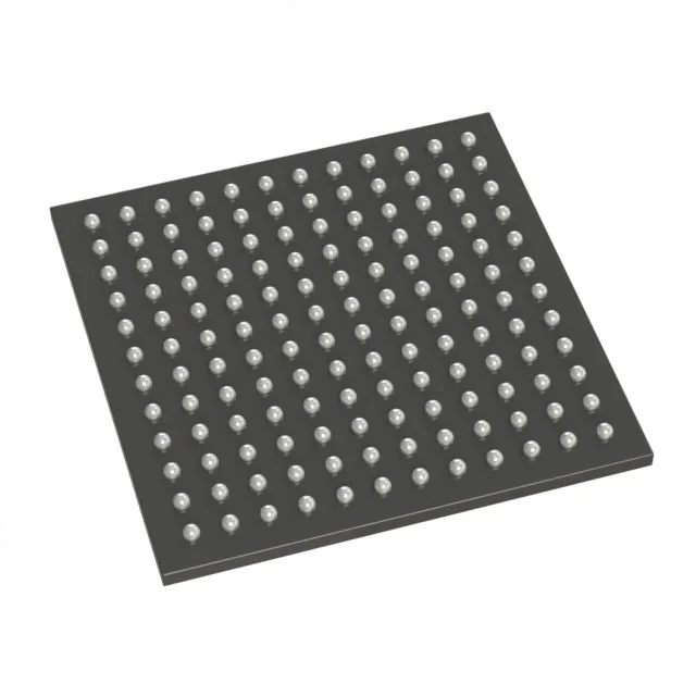
ProASIC3 FPGA – 125K gates in a 144-ball BGA
The Microchip A3P125-FGG144 is a flash-based, non-volatile FPGA from the ProASIC3 series, offering 125,000 system gates and 97 user I/O in a compact 144-ball FPBGA package (13x13 mm). It integrates 36 Kbit of embedded RAM and operates from a 1.5 V core supply (1.425 V to 1.575 V). The flash fabric is live-at-power-up and single-chip – no external configuration memory needed, which simplifies the BOM and improves security. Typical applications include glue logic, I/O expansion, motor control, and industrial sensor interfaces where instant-on and low power matter.
Supply rails and I/O – what the 1.5 V core means for your board
The core voltage is a tight 1.5 V nominal (1.425 V to 1.575 V), so your board needs a dedicated regulator – a 1.5 V LDO or switcher. The I/O banks are separate and can run at 1.5 V, 1.8 V, 2.5 V, or 3.3 V depending on the bank supply voltage you connect. That means the A3P125-FGG144 can interface directly with 3.3 V peripherals on the same die, as long as the I/O bank VCCIO is set to 3.3 V. No level shifters needed for most mixed-voltage designs.
Package and footprint – 144-ball BGA, 1 mm pitch
The 144-FPBGA measures 13x13 mm with a 1 mm ball pitch. That is a four-layer board minimum to route the balls out. The package is surface-mount only – no socket option in production, but a BGA socket adapter exists for prototyping.
Lifecycle – still active, no LTB risk
Microchip lists the A3P125-FGG144 as Active. The ProASIC3 series has been in production for over a decade and remains a staple for cost-sensitive, low-density FPGA applications. If you are qualifying this part for a new design, the active status means you can plan multi-year production without obsolescence-driven respins.
Programming and configuration – JTAG, no external memory
The ProASIC3 fabric is programmed via the JTAG interface. Microchip's FlashPro programmer or third-party tools work. The flash cells retain the configuration on power-off.