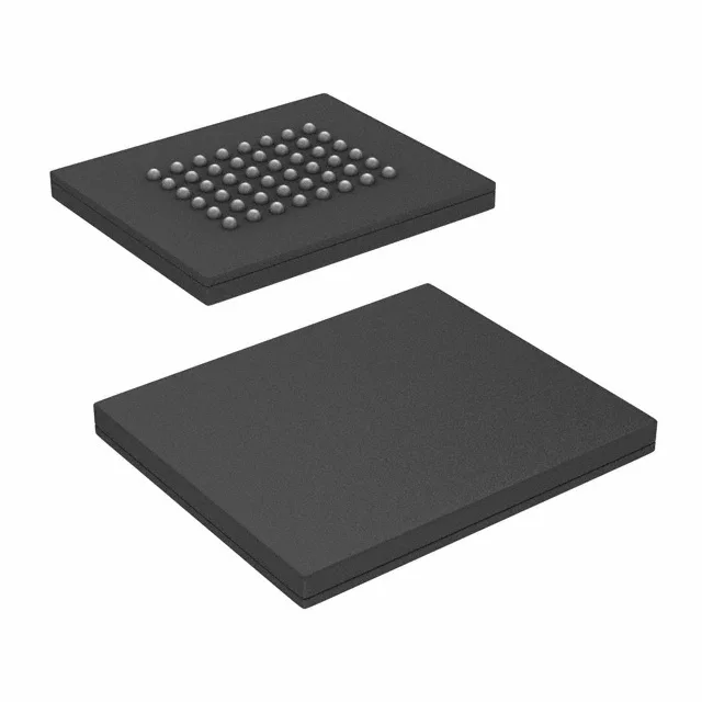
48-FBGA footprint and board-level integration
The S29JL064J70BHI000 ships in a 48-VFBGA package (supplier device package 48-FBGA, 8.15x6.15 mm) — a fine-pitch BGA that demands a controlled solder-paste stencil and X-ray inspection after reflow. The 0.80 mm ball pitch is manageable with standard SMT lines, but the narrow body means the decoupling caps sit close to the package edge; plan for 0402 or 0201 capacitors within 2 mm of the VDD/Q pads to keep the supply impedance below 1 Ω at 70 MHz switching edges.
70 ns access time and parallel interface
This is a 64 Mbit parallel NOR flash with a 70 ns access time — the random-read latency that governs execute-in-place (XIP) performance. At 70 ns the first word appears on the data bus 70 ns after the address is latched; subsequent sequential reads within the same page run at the bus cycle rate. The parallel interface (8-bit or 16-bit wide, organised as 8M x 8 or 4M x 16) lets you match the host bus width without a serial-to-parallel conversion penalty. The write cycle time per word or page is also 70 ns, so page programming at 16-bit width writes 32 bytes in about 2.2 µs.