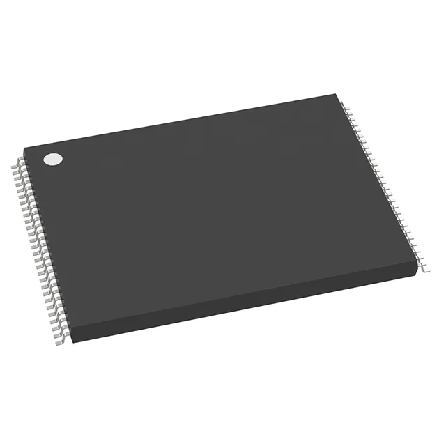
256 Mbit parallel NOR flash with 100 ns access
The S29GL256S10TFIV10: The 100 ns access time sets the ceiling for random read operations — the processor waits one bus cycle per word, so the actual throughput depends on the controller's page-mode burst capability beyond the initial access.
Package and board integration
Housed in a 56-TFSOP package measuring 18.40 mm wide, also designated as 56-TSOP, this is a surface-mount part with a standard 0.50 mm pin pitch. The footprint is shared across the GL-S family — the same board layout accepts the 128 Mbit (S29GL128S10TFIV13) and 512 Mbit (S29GL512T11TFIV20) siblings, giving a straightforward density upgrade path without a PCB respin. The write cycle time for word and page programming is 60 ns, which governs the firmware update speed — a full 256 Mbit erase and reprogram cycle takes on the order of seconds, not milliseconds, so over-the-air update strategies should budget for this latency.
It is fully RoHS3 compliant, which satisfies EU Directive 2015/863 and avoids the restricted-substance paperwork that older non-compliant NOR flashes require.