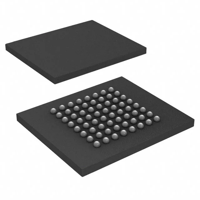
256 Mbit parallel NOR flash in a 64-ball FBGA
The S29GL256S10FHIV20 is a 256 Mbit parallel NOR flash from Infineon's GL-S series, organized as 16M x 16 bits. It delivers a 100 ns access time with a 60 ns word/page write cycle, suiting firmware storage and code-shadowing in embedded systems.
What the 100 ns access time means for the read path
The 100 ns access time governs the initial latency from address assertion to valid data on the bus. In a microcontroller with a parallel memory controller, this sets the maximum wait-state count for zero-wait-state operation — a 100 MHz bus clock (10 ns period) would insert nine wait states per read cycle, so the part is better matched to slower bus clocks or burst-mode controllers that hide the latency behind a cache line fill. The 60 ns word/page write cycle time is the window the controller must hold the write strobe and data valid. Page-mode programming writes up to 256 words in a single operation, amortizing the write overhead across the page size.
Industrial temperature grade and package rework
The 64-ball FBGA (13x11 mm body) with 0.80 mm ball pitch is a hand-reworkable package if you have a hot-air station with a fine nozzle and a stencil for the ball array. The 0.80 mm pitch leaves enough room for a clean solder mask web between pads — less risk of bridging than a 0.50 mm pitch BGA. Pre-bake the part at 125°C for 8 hours if the tray seal was broken, or the absorbed moisture will pop the package during reflow.