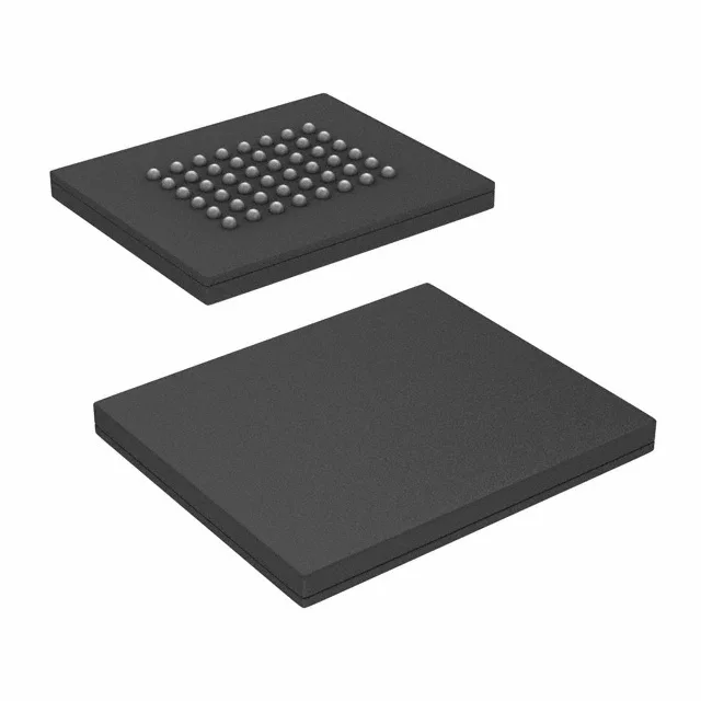
Infineon Technologies S29AL016J70BFI023 — Memory (DRAM / SRAM / Flash / EEPROM)

S29AL016J70BFI023 Infineon 16Mbit Parallel NOR Flash, 70 ns

MPNS29AL016J70BFI023
End of Life

Infineon AL-J series S29AL016J70BFI023 — 16Mbit parallel NOR Flash, 70 ns access time, 2.7V~3.6V supply, 48-VFBGA, -40°C to 85°C.

$2.71Ref. price · indicative, final on quote
Packaging48-VFBGA
StockContact for availability
MOQ1 pcs
  • 100% new & originalTraceable channels only — no refurbs, no pulls, no remarked parts.
  • Date & lot codes on quoteStated per line before you commit; label photos on request.
  • MSL-compliant ESD packingMoisture-sealed bags with indicator cards; reels photo-verified.
  • PayPal buyer protectionPay by T/T, PayPal or Payoneer — card payments covered end to end.

Specifications

S29AL016J70BFI023 Technical Specifications
ParameterValue
SeriesAL-J
Memory typeNon-Volatile
Mounting typeSurface Mount
Voltage2.7V ~ 3.6V
Memory interfaceParallel
Operating temperature-40°C ~ 85°C (TA)
PackageTape & Reel (TR); Cut Tape (CT)
TechnologyFLASH - NOR
Access time70 ns
Memory size16Mbit
Memory formatFLASH
Case48-VFBGA
Memory organization2M x 8, 1M x 16
Write cycle time - word, page70ns

Product details

The Infineon S29AL016J70BFI023 is a 16 Mbit parallel NOR Flash memory from the AL-J series, organized as 2M x 8 or 1M x 16. It delivers a 70 ns access time across the full -40°C to 85°C industrial temperature range, operates from a 2.7 V to 3.6 V supply, and comes in a 48-VFBGA package (8.15 x 6.15 mm footprint). This is the part you reach for when you need a moderate-density code-storage or parameter-logging NOR Flash on a parallel bus — common in industrial controllers, telecom line cards, and embedded systems where the host MCU or FPGA has a parallel memory interface and the firmware image fits within 16 Mbit.

70 ns access time — what it means for the bus

The 70 ns access time is the time from address assertion to valid data on the output pins. The write cycle time is also 70 ns for word and page writes.

16 Mbit density — the BOM-fit tier

16 Mbit (2 MB) is organized as 2M x 8 or 1M x 16.

Frequently asked questions

Can I use S29AL016J70BFI023 as a replacement for S29AL016J70TFI023?

Yes — the S29AL016J70BFI023 and S29AL016J70TFI023 are the same die and same timing (70 ns, 16 Mbit, parallel interface). The only difference is the package: the BFI023 is the 48-VFBGA (BGA), while the TFI023 is the 48-pin TSOP. If your board layout is for TSOP, you cannot drop in the BGA without a PCB redesign; but functionally they are identical.

Is S29AL016J70BFI023 compatible with 3.3V logic?

Yes — the supply range is 2.7 V to 3.6 V, so it operates directly on a 3.3 V rail. All I/O are referenced to VCC, making it compatible with 3.3 V logic families without level translation.

What is the pinout of S29AL016J70BFI023?

The pinout follows the standard 48-ball FBGA footprint for Infineon parallel NOR Flash in this package. The address and data balls are multiplexed depending on the byte/word configuration. The full pin assignment is in the AL-J series datasheet — we do not reproduce the ball map here, but the datasheet is available on request.