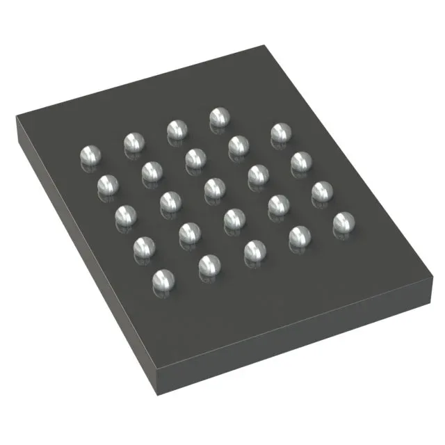
Infineon Technologies S27KS0642GABHI030 — Analog & Data Acquisition

S27KS0642GABHI030 Infineon HyperRAM™ KS 64Mbit PSRAM

MPNS27KS0642GABHI030
End of Life

Infineon HyperRAM™ KS series, S27KS0642GABHI030, 64Mbit PSRAM (Pseudo SRAM), 200 MHz clock frequency, 35 ns access time, HyperBus interface, 1.7V–2V supply, -40°C to +85°C, 24-VBGA surface-mount package.

$5.82Ref. price · indicative, final on quote
Packaging24-VBGA
StockContact for availability
MOQ1 pcs
  • 100% new & originalTraceable channels only — no refurbs, no pulls, no remarked parts.
  • Date & lot codes on quoteStated per line before you commit; label photos on request.
  • MSL-compliant ESD packingMoisture-sealed bags with indicator cards; reels photo-verified.
  • PayPal buyer protectionPay by T/T, PayPal or Payoneer — card payments covered end to end.

Specifications

S27KS0642GABHI030 Technical Specifications
ParameterValue
SeriesHyperRAM™ KS
Memory typeVolatile
Mounting typeSurface Mount
Voltage1.7V ~ 2V
Frequency200 MHz
Memory interfaceHyperBus
Operating temperature-40°C ~ 85°C (TA)
PackageTray
TechnologyPSRAM (Pseudo SRAM)
Access time35 ns
Memory size64Mbit
Memory formatPSRAM
Case24-VBGA
Memory organization8M x 8
Write cycle time - word, page35ns

Product details

HyperRAM™ KS — 64 Mbit PSRAM with HyperBus

The Infineon S27KS0642GABHI030 is a 64 Mbit Pseudo SRAM (PSRAM) from the HyperRAM™ KS family, built around a HyperBus interface that clocks at 200 MHz. It is a volatile memory — data is lost on power-down — but it reads and writes with the simplicity of an SRAM, no refresh overhead visible to the host. The 35 ns access time and 200 MHz clock make it a fit for applications needing fast, dense memory without the cost or pin count of a true SRAM: graphics frame buffers, cache expansion for MCUs, or high-speed data logging in industrial and telecom equipment. The industrial temperature range (-40°C to 85°C) suits outdoor and factory-floor environments.

200 MHz HyperBus and 35 ns access — what they mean for the bus

The 200 MHz HyperBus clock delivers a peak data rate that keeps up with modern MCUs and FPGAs that have a HyperBus controller. The 35 ns access time is the latency from chip-select to first data — fast enough that the memory can serve as a scratchpad or execute-in-place (XIP) memory for code that does not fit in the MCU's internal SRAM. The 8M x 8 organization (64 Mbit) is a single-die density; if the design needs more, the HyperBus protocol supports multiple chip-selects for cascading.

Lifecycle and sourcing

The S27KS0642GABHI030 is listed as Active with ROHS3 compliance.

Frequently asked questions

What is the maximum frequency of S27KS0642GABHI030?

The HyperBus interface runs at 200 MHz, which is the maximum clock frequency for this PSRAM.

Does S27KS0642GABHI030 support 1.8V supply voltage?

Yes — the supply range is 1.7V to 2V, so a 1.8V rail is within spec.

Can I replace S27KS0642GABHI030 with S27KL0642GABHI030?

The S27KL0642GABHI030 is a similar-density part in the same family. Verify the exact memory organization and timing parameters against your design — the S27KL0642 may have different speed grades.