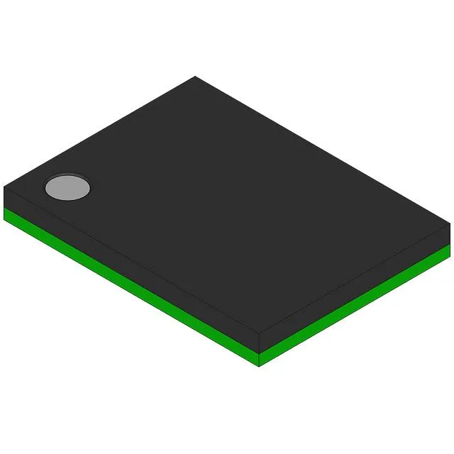
128 Mbit NOR Flash in a 96 ns read window
The S26KL128SDABHB020: That access time is the random-read latency from address to data at the output — the figure that governs how fast the CPU can fetch code on a cache miss. For a 100 MHz MCU with a 10 ns core clock, a 96 ns flash access means the first read stalls for roughly ten cycles before the instruction bus fills.
Housed in a 24-ball PBGA (Plastic Ball Grid Array) package, the footprint is a 6x4 ball array. The 0.80 mm ball pitch keeps the escape routing manageable on a standard four-layer board — no micro-vias required for the outer rows. The BGA package also gives the best signal integrity for the parallel address/data bus by keeping trace lengths short and matched.
Lifecycle and supply posture
Infineon lists the S26KL128SDABHB020 as Active.