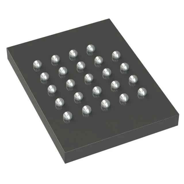
512 Mbit NOR Flash in a 24-BGA — what the FL-S series brings to the board
It communicates over a SPI bus with Quad I/O support, clocked at 133 MHz, which gives it the read throughput to support execute-in-place (XIP) firmware on a host MCU or SoC without needing a separate DRAM staging buffer.
At 133 MHz with Quad I/O, the S25FL512SAGBHIS10 can sustain read throughput well above what single-bit SPI delivers. For a system that boots or executes code directly from flash, that clock speed reduces the number of wait states the CPU sees during instruction fetches. The Quad I/O interface uses four data lines, so the effective data rate is 4 bits per clock cycle. On a 133 MHz bus, that translates to roughly 532 Mbit/s theoretical peak — enough to keep a Cortex-M7 or similar core fed without a cache miss penalty on every branch. The 24-TBGA package (8x6 mm) keeps signal paths short, but the fine-pitch BGA footprint means the PCB layout needs controlled impedance traces and a clean ground plane under the part. X-ray inspection after reflow is recommended to verify solder-joint integrity on the hidden balls.
The FL-S series is well established, and the 24-BGA variant is a standard footprint across multiple density options in the family, so a board designed for this part can scale up or down in density without a layout change.
Package reality — 24-TBGA reflow and handling
The 24-TBGA (8x6 mm) package is a fine-pitch BGA. It is not hand-solderable with a standard iron; rework requires a hot-air station with a BGA nozzle, a stencil for solder paste, and preferably a preheater to avoid thermal shock.