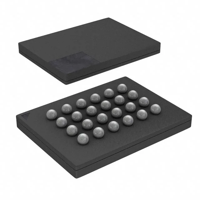
512 Mbit NOR Flash in a 6x8 mm BGA — what the specs mean for the board
The S25FL512SAGBHID10: The 24-ball BGA package (6x8 mm body) saves significant PCB area compared to a 16-pin SOIC, but the fine-pitch BGA requires controlled-depth microvias and X-ray inspection for reliable solder-joint verification in production.
133 MHz Quad-SPI — read throughput and timing margin
The 133 MHz clock frequency on the Quad I/O interface delivers a theoretical read throughput of 532 Mbps (four data lines × 133 MHz). For a firmware-bring-up engineer, this means the MCU can execute code directly from the Flash (XIP) with minimal wait states, provided the host controller supports Quad-SPI at that speed. The 133 MHz rating is the maximum clock; actual throughput depends on the host's SPI controller and the PCB trace length — budget at least 30% timing margin on the data-valid window for production tolerance. At 133 MHz, signal integrity on the four data lines matters: keep each trace matched within ±5 mm and avoid vias on the clock line if possible.
Supply range and power rail compatibility
This margin handles the drop across a Schottky diode or a 3.3 V LDO with 200 mV dropout at full load. For a power-rail design review, the part draws its peak current during a program or erase cycle — the datasheet's active current spec (not in the ledger, but typical for this density) should be factored into the 3.3 V regulator's load budget. The wide range also allows operation from a 3.0 V battery during backup, though the 133 MHz speed is guaranteed only down to 2.7 V.
The 85°C ceiling is the standard industrial grade; if your design must survive sustained 105°C ambient (e.g., under-hood or near a motor drive heatsink), the S25FL512SAGBHV210 sibling extends the range to 105°C in the same BGA footprint.
The part is ROHS3 compliant.