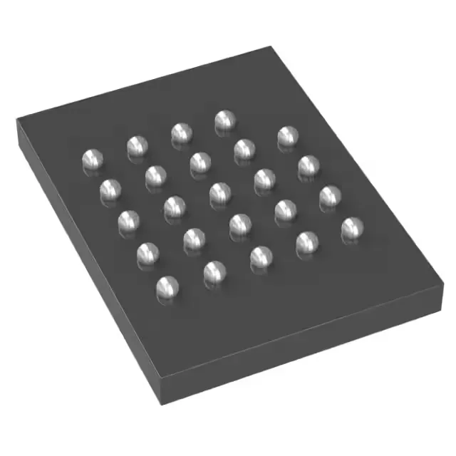
Infineon Technologies S25FL512SAGBHI213 — Memory (DRAM / SRAM / Flash / EEPROM)

Infineon S25FL512SAGBHI213 512Mbit NOR Flash

MPNS25FL512SAGBHI213
End of Life

Infineon FL-S series 512 Mbit NOR flash, 64M x 8 organization, 133 MHz SPI Quad I/O, 2.7–3.6 V, -40°C to 85°C, 24-TBGA (8x6 mm) tape-and-reel.

$8.6625Ref. price · indicative, final on quote
Independent supplier — new & surplus stockAuthenticity-screened · ESD-safe packingListing updated Aug 2026

Specifications

S25FL512SAGBHI213 specifications
ParameterValue
SeriesFL-S
Memory typeNon-Volatile
MountingSurface Mount
Supply voltage2.7V ~ 3.6V
Clock frequency133 MHz
Memory interfaceSPI - Quad I/O
Operating temperature-40°C~85°C(TA)
PackageTape & Reel (TR)
TechnologyFLASH - NOR
Memory size512Mbit
Memory formatFLASH
Case24-TBGA
Memory organization64M x 8

Product details

The Infineon S25FL512SAGBHI213 is a 512 Mbit NOR flash from the FL-S family, organized as 64M x 8, communicating over an SPI Quad I/O interface clocked at 133 MHz. That clock rate means the part can sustain a read throughput high enough to support execute-in-place (XIP) for a modern MCU or FPGA configuration image without stalling the core.

24-ball BGA — footprint and reflow considerations

The solder-ball layout demands a clean PCB land pattern and a reflow profile that matches the JEDEC MSL level for this package. The compact footprint saves board area, but the BGA makes post-assembly inspection and rework harder than a QFP — something to factor into the manufacturing yield plan.

For a production BOM, this reduces the supply-chain risk of a sudden discontinuation.

Frequently asked questions

What is the memory organization of S25FL512SAGBHI213?

The memory is organized as 64M x 8 bits — that is 512 megabits total, arranged in a single 8-bit-wide array. The SPI Quad I/O interface accesses the array in page, sector, or block granularity.