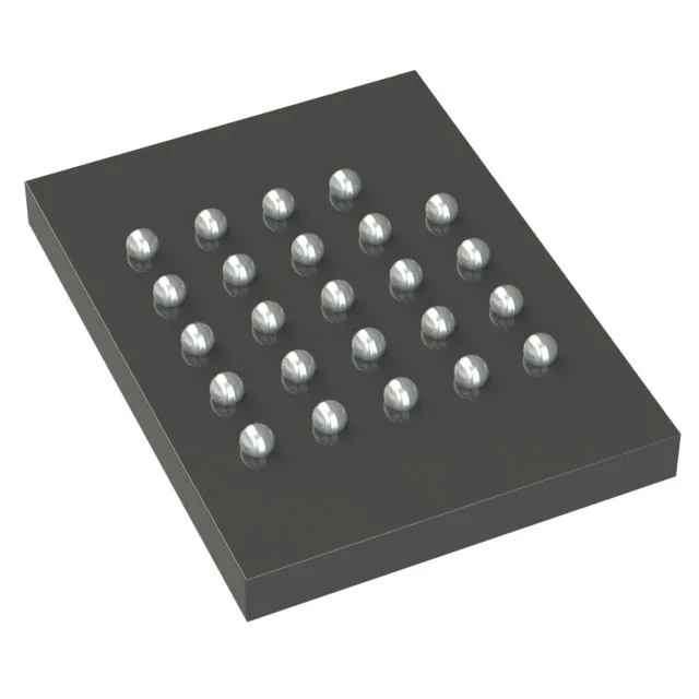
512 Mbit NOR Flash for automotive-grade code storage
The Cypress S25FL512SAGBHBA10 is a 512 Mbit non-volatile NOR Flash memory from the Automotive, AEC-Q100 FL-S series, organized as 64M x 8 bits. It communicates over a SPI interface with Quad I/O support at a clock frequency of 133 MHz, which provides the read throughput needed for execute-in-place (XiP) firmware and fast over-the-air update staging in automotive ECUs.
AEC-Q100 grade and 105°C operating range — the qualification envelope
The 105°C ceiling is the typical boundary for engine-adjacent electronics that see underhood soak but stay below the hottest exhaust-side zones. If your program requires 125°C operation, the sibling S25FL512SAGMFMG10 carries that extended range in a different package. The 2.7V to 3.6V supply range matches standard 3.3V automotive power rails and provides margin for cold-crank dips down to 2.7V.
24-ball BGA (8x6 mm) — footprint and rework considerations
This contrasts with the SOIC-16W package of the S25FL512SAGMFBG10 sibling, which is easier to hand-solder and inspect. The BGA saves board area but adds a rework step if a device must be replaced in a rework lab.
133 MHz Quad-SPI — bus margin for XiP and fast reads
The 133 MHz clock rate with Quad I/O yields a theoretical read throughput of 532 Mbps (four data lines at 133 MHz). In practice, the firmware team should budget for one or two wait states at the memory controller when running the SPI bus at full speed, especially across temperature. The Quad-SPI interface also supports memory-mapped read modes that let the host CPU execute code directly from the Flash without copying to RAM.