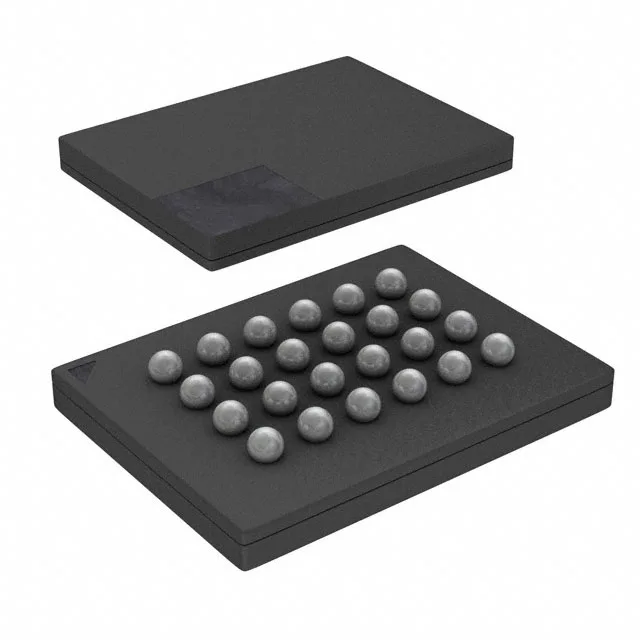
256 Mbit NOR Flash on a 133 MHz Quad-SPI bus
That clock rate, combined with the quad data lines, gives a sustained read throughput that keeps a Cortex-M or application processor fed during execute-in-place (XIP) or shadow-to-RAM boot sequences. The 24-ball BGA package (6x8 mm body) saves board area compared to an SOIC-16 wide-body, but demands careful PCB layout for the fine-pitch balls and thermal management.
133 MHz clock — what it buys the system
The Quad I/O interface uses four data lines plus a clock and chip select, keeping the signal count to six traces. The 256 Mbit density holds a full Linux kernel, a file system, or a year's worth of data-log entries. NOR Flash also supports random-access reads, so the MCU can execute code directly from the device without copying it to RAM first — useful in cost-sensitive designs where the internal SRAM is small.
Cypress lists the S25FL256SAGBHID10 as Active. For a procurement team qualifying a new BOM, this part carries no near-term obsolescence risk. The FL-S series has broad distribution coverage, so lead times and pricing are competitive — confirm current availability at quote time through your sourcing channel.
BGA footprint — layout and rework notes
The 24-BGA (6x8 mm) package uses a 0.8 mm ball pitch typical of small-outline BGA memories. The PCB land pattern should follow the supplier's recommended pad diameter (usually 0.35 mm NSMD) and a solder mask defined pad. A 0.1 mm thick stencil with 0.4 mm aperture openings gives a consistent solder volume. During rework, pre-bake the board at 125°C for 4 hours if the moisture-sensitive level (MSL 3) floor life has been exceeded — the BGA body absorbs moisture faster than a SOIC. Decouple the supply pins with a ceramic capacitor placed as close to the BGA balls as the via pattern allows.