256 Mbit NOR Flash with Quad-SPI for firmware and data storage
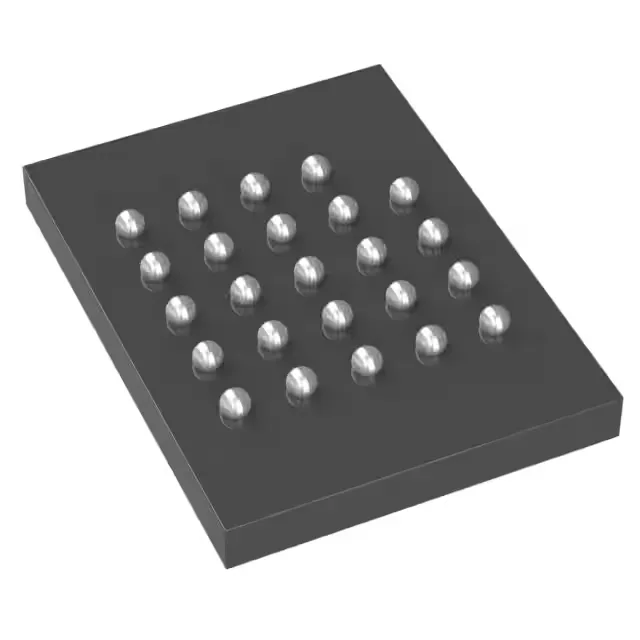
The S25FL256LAGBHI023: It uses a SPI interface with Quad I/O and QPI support, clocked at 133 MHz for fast read throughput. It comes in a 24-ball BGA package measuring 8x6 mm, suitable for surface-mount assembly in space-constrained designs. Typical applications include firmware storage, boot code, configuration data, and OTA update staging in embedded systems, industrial controllers, networking equipment, and IoT edge nodes.
133 MHz Quad-SPI — what it means for read bandwidth
The 133 MHz clock frequency applies to the Quad I/O and QPI modes, where four data lines transfer one byte per clock cycle. This yields a theoretical read throughput of 532 Mbps (133 MHz × 4 bits), which significantly reduces firmware load times compared to standard SPI at the same clock. For designs that need to execute code in place (XIP) from external Flash, the Quad-SPI interface keeps the memory bus from becoming a bottleneck. The 2.7V to 3.6V supply range is compatible with common 3.3V logic families, and the 256 Mbit density provides 32 MB of storage — enough for complex firmware images with room for a fallback recovery partition.
24-BGA footprint and assembly considerations
The 24-ball BGA package (supplier device package 24-BGA, 8x6 mm) requires a standard BGA reflow profile with MSL level per the component marking. For layout, follow the manufacturer's recommended land pattern and keep the decoupling capacitors close to the supply balls. The industrial temperature range covers most outdoor and factory-floor environments, but if the design sees sustained junction temperatures above 85°C, consider the automotive-grade variant S25FL256LAGMFM003 rated to 125°C.