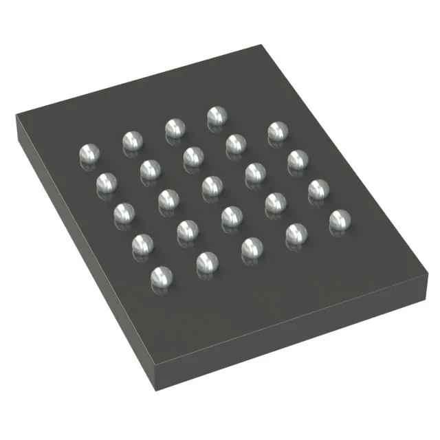
128 Mbit NOR Flash in a 24-ball BGA — what this part is for
The Infineon S25FL128SDSBHI210 is a 128 Mbit FL-S series NOR Flash memory with an SPI and Quad I/O interface, clocked at 80 MHz. It stores firmware, configuration tables, or boot code in embedded systems that need fast random-access read and reliable non-volatile storage.
80 MHz Quad-SPI — read throughput for code shadowing
The same die in the S25FL128SAGBHIA10 and S25FL128SAGMFV010 variants runs at 133 MHz, so if your processor's SPI port tops out above 80 MHz and the layout can handle the faster edge rates, those parts recover about 40% more bandwidth. For designs already limited by the host SPI clock or trace length, the 80 MHz part avoids any signal-integrity margin squeeze.
24-ball BGA — footprint and rework considerations
The 24-TBGA package (8x6 mm body) saves board area compared to an SOIC or WSON, but the BGA footprint demands at least a four-layer PCB with microvia or blind-via escape routing under the balls. Reflow profile follows standard lead-free SAC305; X-ray inspection is needed to verify solder-joint integrity after assembly. The S25FL128SDSNFI000 alternative uses a WSON package with exposed pad, which is easier to hand-solder and inspect but takes more board space.
That means Infineon continues to manufacture it without a published last-time-buy or end-of-life notice.