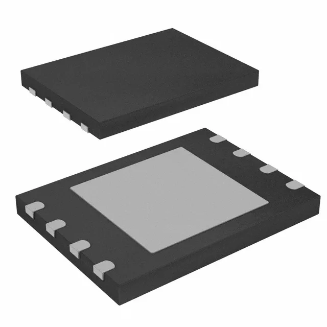
Infineon Technologies S25FL128SAGNFI003 — Memory (DRAM / SRAM / Flash / EEPROM)

Infineon S25FL128SAGNFI003 128Mbit NOR Flash, SPI Quad I/O, 133 MHz

MPNS25FL128SAGNFI003
End of Life

Infineon (Cypress) FL-S series 128Mbit NOR flash, SPI Quad I/O interface, 133 MHz clock, 2.7V–3.6V supply, -40°C–85°C operating temperature, 8-WDFN exposed-pad (6×8mm), 16M×8 organization.

$4.6400Ref. price · indicative, final on quote
Independent supplier — new & surplus stockAuthenticity-screened · ESD-safe packingListing updated Aug 2026

Specifications

S25FL128SAGNFI003 specifications
ParameterValue
SeriesFL-S
Memory typeNon-Volatile
MountingSurface Mount
Supply voltage2.7V ~ 3.6V
Clock frequency133 MHz
Memory interfaceSPI - Quad I/O
Operating temperature-40°C~85°C(TA)
PackageTape & Reel (TR); Cut Tape (CT)
TechnologyFLASH - NOR
Memory size128Mbit
Memory formatFLASH
Case8-WDFN Exposed Pad
Memory organization16M x 8

Product details

The part operates from a 2.7 V to 3.6 V supply and is rated for -40°C to 85°C, covering industrial and outdoor telecom enclosures.

133 MHz clock — what it means for read throughput

The 133 MHz clock rate supports execute-in-place boot without wait states on a moderate-speed bus. Throughput depends on the controller's SPI peripheral and dummy cycle count.

Lifecycle status — what the record shows

The lifecycle stage field flags this part as eol_hot, while the product status field shows Active. Confirm the current lifecycle status with your distributor at quote time.

Package and mounting — 8-WSON with exposed pad

The 8-WDFN exposed-pad package (6 × 8 mm) is a surface-mount, no-lead footprint.

Frequently asked questions

What is the supply voltage range and does it work on a 3.3 V rail?

The S25FL128SAGNFI003 operates from 2.7V to 3.6V, which covers the standard 3.3 V nominal rail with typical ±5% tolerance. No new rail is required for most legacy designs already using 3.3 V; confirm the board's worst-case rail tolerance stays above 2.7 V under all load conditions.

What does the 8-WDFN exposed-pad package mean for board-level rework?

The exposed paddle under the 8-WSON (6×8 mm) die pad must be soldered to the board landing pad for rated thermal performance. Desoldering requires preheat to avoid cracking the WDFN body; hot-air rework with a calibrated temperature profile is standard. The landing pad and thermal via stack-up are datasheet-specified — confirm the boardfab stack-up matches before assembly.

What is the lead time for a production-order quantity?

With lifecycle_stage at eol_hot, lead time is governed by the remaining authorized channel inventory plus the LTB window — both must be confirmed via RFQ. Open-market surplus lots may appear at shorter lead times but require Certificate of Conformance and incoming inspection to validate Quad I/O endurance and erase-cycle count.