64 Mbit NOR Flash with 108 MHz Quad SPI — what this means for your design
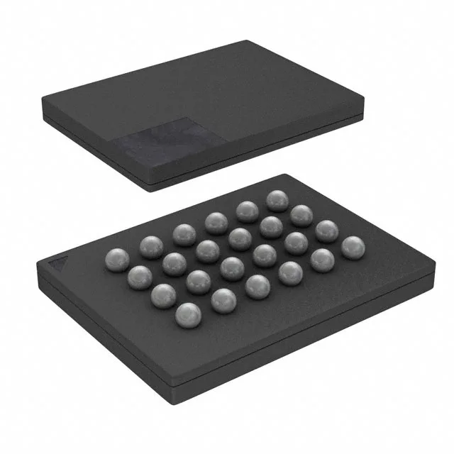
It communicates over a SPI interface that supports Quad I/O and QPI protocols, pushing the clock frequency to 108 MHz. That Quad I/O mode lets you read four data bits per clock cycle, so the effective throughput is well above what a standard SPI part delivers at the same clock — useful for shadowing code into RAM or storing configuration tables in an industrial controller. Packaged in a 24-ball BGA (6x8 mm body), it takes up roughly the same board area as a SOIC-8 but with a finer ball pitch. That BGA footprint saves space but means the rework profile needs care — more on that below.
24-ball BGA footprint — what the rework bench sees
The 24-BGA package measures 6x8 mm with a ball pitch fine enough that a standard hot-air rework station can handle it, but the profile matters. The BGA pads are underneath; a via-in-pad layout needs proper tenting or fill to avoid solder wicking. The thermal pad (if present) should be stitched to a ground plane with several vias to pull heat away during continuous read bursts.