100 V, 75 A — the OptiMOS 6 sweet spot for 48 V and 24 V bus rails
The ISC080N10NM6ATMA1 is an N-channel enhancement-mode MOSFET from Infineon's OptiMOS 6 trench technology family, rated 100 V drain-source and 75 A continuous drain at the case (Tc). The 100 V breakdown gives enough headroom for 48 V telecom rectifiers, 48 V server racks, and 24 V industrial bus rails with margin for load-dump transients — the nominal rail sits well below the 100 V ceiling.
8.05 mOhm Rds(on) — the conduction loss floor at 75 A
Maximum on-resistance is 8.05 mOhm at 20 A drain current with 10 V gate drive — this is the nominal Rds(on) at the recommended gate voltage. At 75 A continuous drain, conduction loss at this Rds(on) is roughly 45 W (I²R) — the 100 W case-rated power dissipation (Tc) can handle that, but the 3 W ambient-rated dissipation (Ta) means the board-level copper and airflow must pull the heat out. Gate drive voltage is specified between 8 V and 10 V for minimum Rds(on) — driving at 10 V ensures the channel is fully enhanced; driving at 8 V saves a little gate-drive loss but leaves a few percent higher on-resistance.
24 nC gate charge — switching loss scales linearly with Qg
Total gate charge at 10 V is 24 nC typical — for a 100 V, 75 A MOSFET this is a low Qg figure, which directly reduces the gate-driver current needed at a given switching frequency. Input capacitance Ciss is 1800 pF at 50 V drain-source — this sets the Miller plateau charge and the switching speed limit; a 1 A gate driver can charge this capacitance in about 1.8 ns, but the practical switching edge is limited by the gate loop inductance and the driver's peak current. The 1800 pF Ciss at 50 V is lower than many competing 100 V MOSFETs in this current class, which means lower switching losses in hard-switched topologies like synchronous buck converters and half-bridge stages.
PG-TDSON-8 FL — the thermal path through the exposed pad
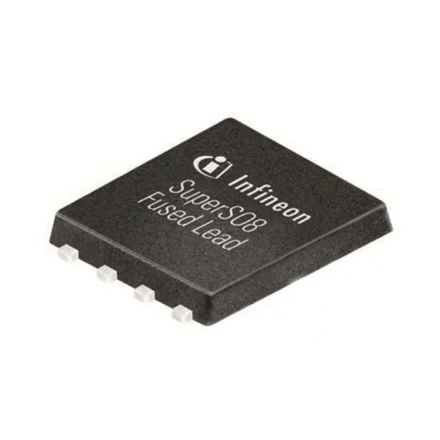
The 8-PowerTDFN package (PG-TDSON-8 FL) has a large exposed drain pad on the bottom — the thermal resistance to case is specified at 100 W dissipation, so the PCB copper plane under the pad is the primary heat path. Surface-mount assembly with standard reflow profiles; the exposed pad requires a thermal via array under the package to pull heat into the inner-layer copper planes — a 2-oz copper pour with at least 16 vias is typical for the 75 A continuous rating. Operating junction temperature range is -55 °C to 175 °C — the 175 °C max is the silicon limit; derate the continuous current above 100 °C case temperature per the datasheet's SOA curve.