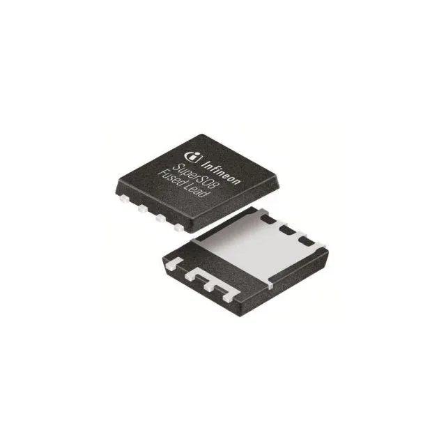
The Infineon ISC012N04LM6ATMA1 is a 40 V N-channel MOSFET from the OptiMOS™ 6 trench family, built for high-efficiency switching in power conversion and motor-drive stages. Its headline figure is a 1.2 mOhm maximum on-resistance at 50 A drain current with 10 V gate drive — that conduction loss stays under 3 W even at 50 A, which keeps the heatsink small in a 48 V bus converter or an automotive 12 V load switch. The 238 A continuous drain rating at case temperature (Tc) tells you the silicon can handle massive current if you pull the heat out through the exposed pad; the 37 A at ambient (Ta) is the real-world limit on a bare PCB without forced air.
Rds(on) and gate drive — matching the driver to the MOSFET
The 1.2 mOhm figure is specified at 10 V gate drive, but the part also lists a 4.5 V drive voltage for minimum on-resistance — that means a logic-level gate driver can still turn it on hard, though the Rds(on) will be higher than the 10 V value. Check the gate charge curve: 64 nC at 10 V means the driver needs to source and sink that charge fast enough to keep switching losses under control at the target frequency. Input capacitance is 4600 pF at 20 V drain-source — a typical 1 A gate driver will charge it in about 30 ns, which is fine for 100 kHz to 200 kHz hard-switched converters. If you are paralleling multiple devices, the 64 nC Qg and 4600 pF Ciss are low enough that gate-resistor tuning is straightforward.
PG-TDSON-8 FL — rework and footprint notes
The 8-PowerTDFN package (PG-TDSON-8 FL) is a 5 mm × 6 mm body with an exposed die pad on the bottom. Rework with hot air is doable: preheat the board to 125°C, hit the pad with 280°C air until the solder reflows, then lift with tweezers. The pad is large enough that alignment marks are clear, and the package has a small index notch. Keep the stencil aperture at 80% of the pad area to avoid solder bridging to the drain pins.
Active lifecycle — no obsolescence clock ticking
The OptiMOS 6 series is Infineon's latest trench MOSFET generation, so a successor is not expected in the near term. For dual-sourcing, Infineon's own portfolio includes other 40 V OptiMOS 6 variants in the same PG-TDSON-8 FL footprint, but the 1.2 mOhm Rds(on) is specific to this part number — verify pin compatibility if cross-referencing.