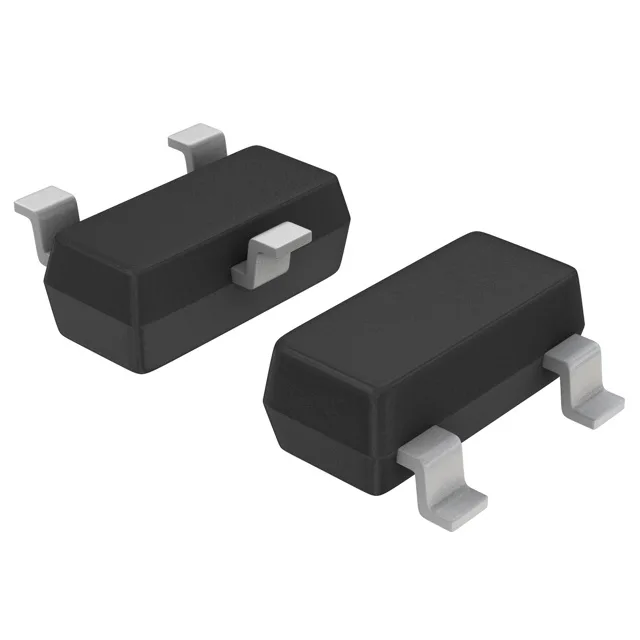
Logic-level switch in a SOT-23 — what it can and cannot do
The 1.3 W power dissipation at ambient temperature (Ta) is the real thermal ceiling. At 6.3 A the conduction loss alone (I²R) hits 0.83 W, leaving little headroom for switching losses or elevated ambient. For any continuous load above 4 A, plan on a copper pour under the SOT-23 pad to pull heat into the board.
Gate drive thresholds — what 1.8 V logic means
The drive voltage range is specified from 2.5 V (minimum for rated Rds(on)) up to 4.5 V (maximum Rds(on) condition). The maximum gate threshold is 1.1 V at 10 µA drain current, which means the FET starts turning on well below 2.5 V — but at 1.8 V gate drive the on-resistance will be significantly higher than the 21 mOhm at 4.5 V. For a 1.8 V logic rail, expect several hundred milliohms and derate the current accordingly. Gate charge is 8.9 nC at 4.5 V, and input capacitance is 700 pF at 16 V drain-source. These are low enough that a GPIO pin can drive the gate directly at moderate switching frequencies (tens of kHz). Above 100 kHz the gate drive current from the logic output becomes a limiting factor.