Gate drive and switching parasitics
Total gate charge is 18.7 nC at Vgs = 10 V, and input capacitance (Ciss) is 433 pF at Vds = 100 V — numbers that keep the gate drive requirements modest for a 500 V device. A typical 1 A gate driver can switch this MOSFET in under 20 ns, which is fast enough for hard-switching topologies up to the low hundreds of kHz. That 13 V sweet spot means a standard 12 V bias rail with a small boost regulator or a dedicated 13 V gate-drive supply is the right call — a straight 12 V rail leaves a few milliohms of Rds(on) on the table.
Thermal budget in the full-pack package
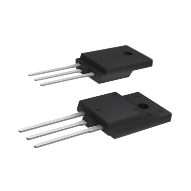
The full-pack construction puts a molded resin layer between the die and the mounting surface, so the thermal resistance junction-to-case is higher than a standard TO-220 — budget the heatsink accordingly. At 11.1 A and 500 mOhm, conduction loss alone is over 60 W at 25 °C junction, so the 28 W dissipation ceiling means the part is thermally limited well before the current rating in any real application.
Last Buy — plan the BOM transition
This is not an NRND or a slow phase-out — it is the final purchasing window before the part is discontinued. If this MOSFET is on your BOM, the next step is to secure last-time-buy quantities or qualify a replacement before the order window closes. The CoolMOS family includes many 500 V N-channel devices in TO-220FP, but a pin-compatible drop-in with the same Rds(on) and gate charge profile would need to be evaluated against the specific switching frequency and drive voltage in your design.