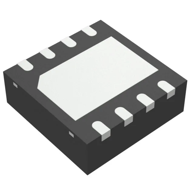
The Cypress FM25V20A-DGQ is a 2 Mbit non-volatile FRAM (ferroelectric RAM) memory IC organized as 256K x 8 bits, accessed through an SPI serial interface at clock frequencies up to 40 MHz. FRAM technology combines the non-volatility of EEPROM with the write speed and endurance of SRAM — writes complete immediately with no write-cycle delay, and the part is rated for 10^14 read/write cycles, eliminating the wear-leveling logic needed with Flash.
For new designs this removes the supply-chain risk of a phase-out during the product's production run. If you are qualifying a BOM for a multi-year production program, this part's active status and RoHS compliance reduce the compliance documentation burden.
Package and footprint — 8-DFN with exposed pad
The package is surface-mount only; the Tube shipping medium means the part arrives in a standard antistatic tube for pick-and-place or manual assembly. No reel or tape quantities apply for this variant, so plan for tube-handling on the line or transfer to tape if your feeder requires it.
SPI interface — no dead cycles, no polling
The SPI interface supports read and write operations at the full 40 MHz clock with no write-cycle delay — a key distinction from serial EEPROM and Flash, which require a polling loop or a write-complete wait. For a 2 Mbit (256K x 8) memory, a full-chip read at 40 MHz takes roughly 6.4 ms; a full-chip write takes the same time because each byte is written immediately. This makes the part suitable for high-frequency data logging, parameter storage, and configuration snapshots where the write latency of Flash would stall the system. The SPI bus is compatible with standard SPI masters, including those on MCUs from ST, NXP, Microchip, and TI.