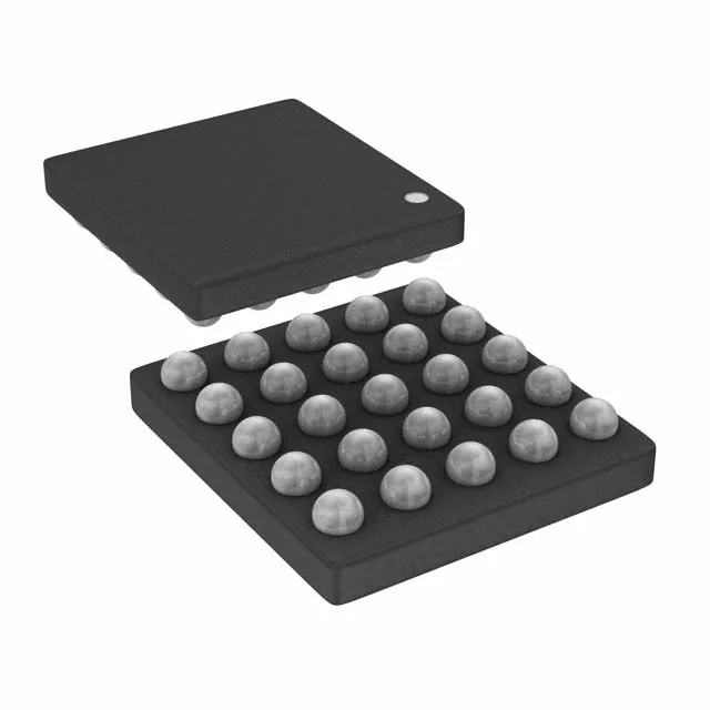
Infineon Technologies CY8C4745FNI-S412T — Logic ICs

CY8C4745FNI-S412T PSoC 4 MCU, ARM Cortex-M0+, 48 MHz

MPNCY8C4745FNI-S412T
End of Life

Infineon PSoC® 4 CY8C4700S series, CY8C4745FNI-S412T, ARM® Cortex®-M0+ 32-Bit MCU, 48 MHz, 32 KB Flash, 4K x 8 RAM, 21 I/O, I²C/SPI/UART, CapSense, -40 to 85°C, 25-WLCSP.

$6.48Ref. price · indicative, final on quote
Packaging25-XFBGA, WLCSP
StockContact for availability
MOQ1 pcs
  • 100% new & originalTraceable channels only — no refurbs, no pulls, no remarked parts.
  • Date & lot codes on quoteStated per line before you commit; label photos on request.
  • MSL-compliant ESD packingMoisture-sealed bags with indicator cards; reels photo-verified.
  • PayPal buyer protectionPay by T/T, PayPal or Payoneer — card payments covered end to end.

Specifications

CY8C4745FNI-S412T Technical Specifications
ParameterValue
SeriesPSOC® 4 CY8C4700S
Mounting typeSurface Mount
Oscillator typeInternal
Program memory typeFLASH
Voltage - supply (Vcc (Vdd))1.71V ~ 5.5V
Operating temperature-40°C ~ 85°C (TA)
Speed48MHz
PackageTape & Reel (TR); Cut Tape (CT)
RAM size4K x 8
Core size32-Bit Single-Core
PeripheralsBrown-out Detect/Reset, CapSense, LCD, LVD, POR, PWM, WDT
ConnectivityI²C, IrDA, LINbus, Microwire, SmartCard, SPI, SSP, UART/USART
Number of i (O)21
Core processorARM® Cortex®-M0+
Case25-XFBGA, WLCSP
Data convertersA/D 16x10b
Program memory size32KB (32K x 8)

Product details

48 MHz Cortex-M0+ in a 2 mm x 1.93 mm WLCSP — the space-constrained touch-and-display MCU

The Infineon CY8C4745FNI-S412T is a PSoC 4 family MCU built around a 32-bit ARM Cortex-M0+ core clocked at 48 MHz. The supply voltage range spans 1.71 V to 5.5 V, so it can run from a single Li-ion cell or a regulated 3.3 V / 5.0 V rail without an external LDO. On-chip peripherals include a 16-channel 10-bit ADC, brown-out and low-voltage detect, POR, PWM timers, and a watchdog timer.

WLCSP rework and handling notes

The 25-WLCSP package has a 0.4 mm ball pitch typical for this class. The small body means the die is close to the board surface, so the reflow profile needs a controlled ramp rate to avoid thermal shock. The 21 GPIOs are all that fit in the 25-ball array. For designs needing more I/O, the QFN-packaged siblings in the same PSoC 4 family offer 34 or 36 I/O in a larger footprint.

Lifecycle and compliance

It is ROHS3 compliant.

Frequently asked questions

What is the pinout of CY8C4745FNI-S412T?

Design engineers need pinout for PCB layout and proper signal routing.

What is the price of CY8C4745FNI-S412T?

Sourcing buyers compare prices to meet BOM cost targets.

Where can I buy CY8C4745FNI-S412T in stock?

Buyers need immediate availability to avoid production delays.

Is CY8C4745FNI-S412T obsolete or active?

Brokers and buyers confirm lifecycle to avoid supply chain risk.

What is the difference between CY8C4745FNI-S412T and CY8C4745AZI-S412?

Engineers compare package variants to choose the correct part for layout constraints.

What is the equivalent for CY8C4745FNI-S412T?

When the exact part is unavailable, cross-referencing finds drop-in alternatives.